SEMICONDUCTOR ELECTRONICS : MATERIALS, DEVICES AND SIMPLE CIRCUITS
SOLIDS
All solids are made up of atoms and molecules but due to different arrangement of the molecules inside them, they are divided into two classes (a) crystalline and (b) amorphous.
PROPERTIES OF CRYSTALLINE SOLIDS
- The atoms and molecules are arranged in a definite or regular order.
- Crystalline solids are bounded by flat surfaces.
- They possess uniform chemical composition.
- They have sharp melting point.
- They are anisotropic.
- They have symmetry.
PROPERTIES OF AMORPHOUS SOLIDS
- The atoms and molecules are arranged in an irregular manner.
- These are isotropic i.e. they have same physical properties in all directions.
- They do not have a sharp melting point.
- They do not have any symmetry.
CRYSTAL LATTICE
It is defined as the infinite array of atoms and molecules in space (three dimensions) such that at every point, an atom or the molecule has got the identical surroundings.
LATTICE VECTORS
Let a and b be the distance between the two successive atoms (points) of the lattice along the x-axis and y-axis, then the lattice vector is given by
For three dimensional lattice, 
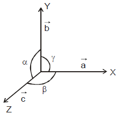
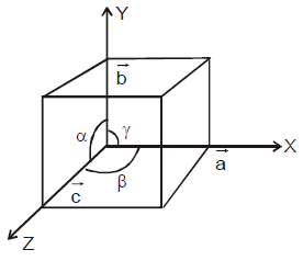
LATTICE PARAMETERS
In a three dimensional crystal structure, the translational vectors  along the x, y and z axis and the angles (α, β and γ) in between the translational vectors are called lattice parameters.
UNIT CELL
A unit cell is the smallest geometrical unit in three dimensions. The repetition of which will give the entire crystal. The crystalline solid is said to be consisting of a large no. of unit cells, each one in contact with immediate neighbours.
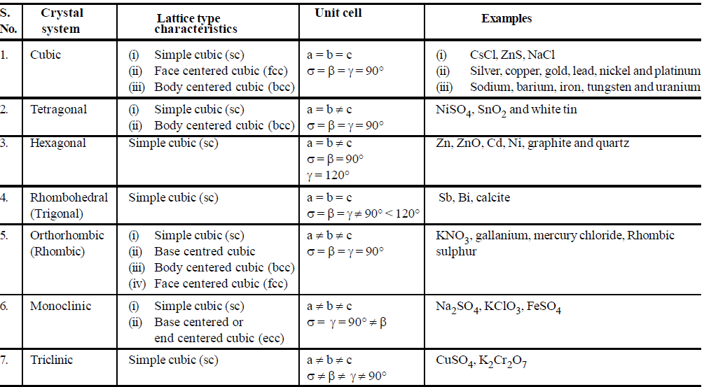
CRYSTAL SYSTEM
Based on the different combination of lattice parameters (a, b, c) and the angles (α, β and γ) we can define crystal system as follows.
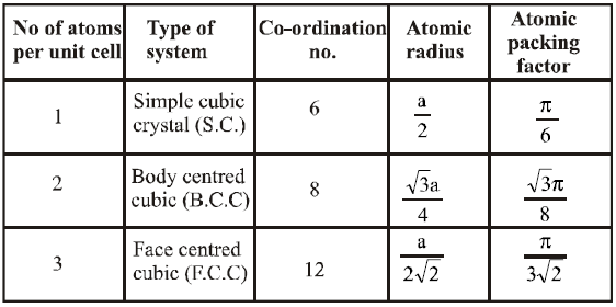
CHARACTERISTICS OF THE UNIT CELL OF A CUBIC SYSTEM
- Volume of a unit cell (V) = (a × b × c) or V = a × b × c
- Mass and density of a unit cell :
The mass of unit cell = number of atoms or molecules in the cell × mass of each atom
or, m = p × ma or  where M = molecular wt. of the substance
∴ density 
If edge a, is given in picometre then
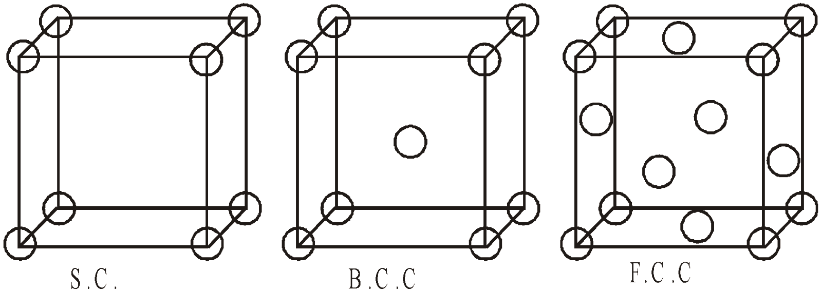
- Number of atoms (N) in a unit cell or the total number of atoms per unit cell is given by

where Ni = no. of body centred or interior atoms
Nf = no. of face centered atoms
Nc = no. of corner atoms.
COORDINATION NUMBER
The number of nearest neighbours of a given atom in the crystal is called the coordination number.
Half of the distance between the centres of two neighbouring atoms is called atomic radius. It is also called lattice constant or lattice parameter.
ATOMIC PACKING FACTOR OR DENSITY OF PACKING
It is defined as ratio of the volume occupied by all the atoms in a unit cell to the total volume of the unit cell.
ENERGY BAND THEORY OF SOLIDS
When two identical atoms, are far apart, the electronic levels (or electronic wave functions) in one are not disturbed by the presence of other atom fig 1(a). For example, the 3s electron of each sodium atom has a single energy with respect to its nucleus. But when the two atoms come closer, these electron’s wave function starts to overlap and each electron revolves round both nuclei.
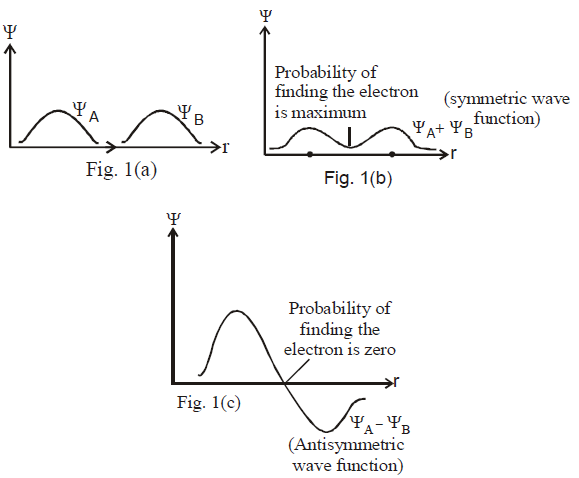
Fig. 1 : Wave functions of two sodium atoms (each in G-state) :
(a) At wide separation
(b) Small separation : Isolated wave function combined with same sign (i.e., lower energy)
(c) Small separation : Isolated wave function combined with opposite sign i.e., antisymmetric state of joint wave functions ΨA & ΨB(higher energy state)
Splitting of 3s levels when two atoms are brought together.
Splitting of 3s levels when four atoms are brought together.
Formation of 3s band by a larger number of atoms.(G-state)
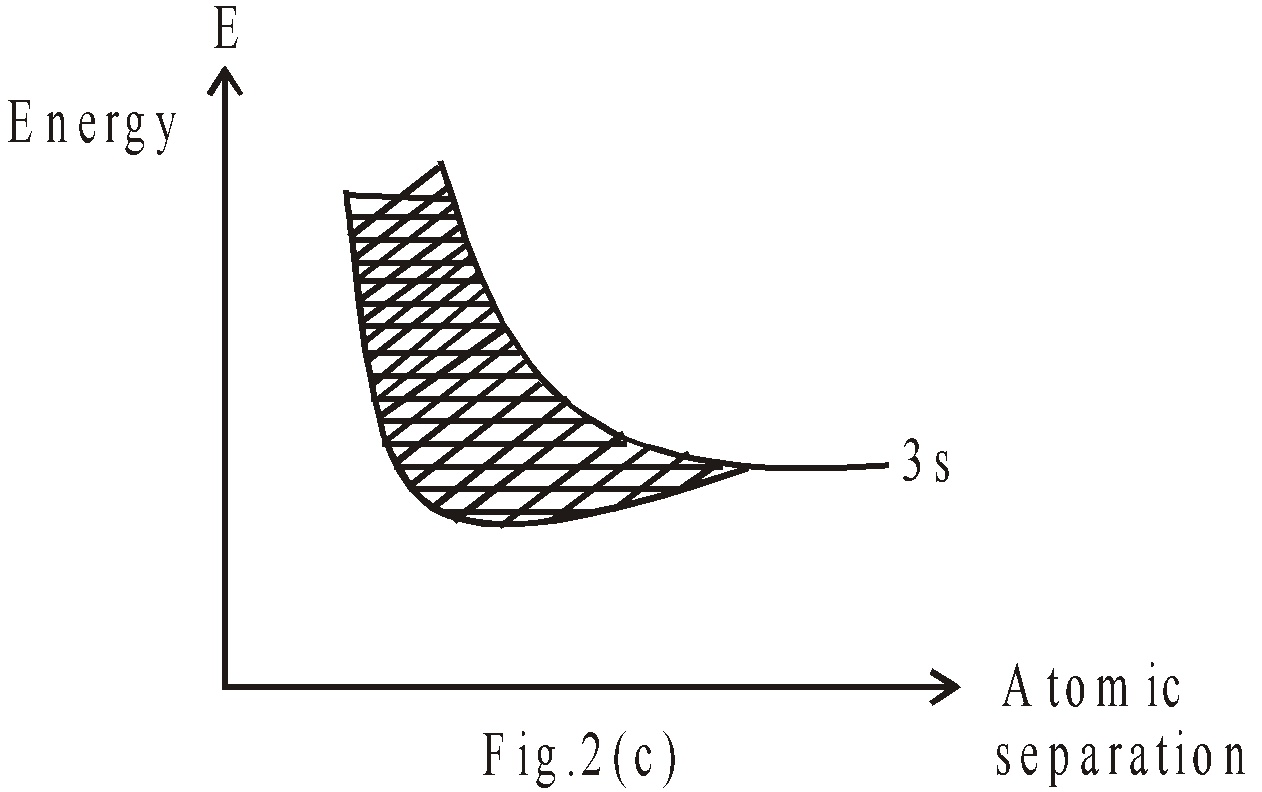
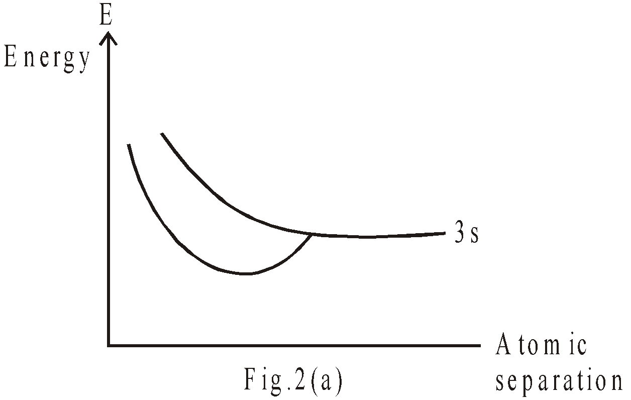
The wave function of each electron is roughly, a combination of the wave functions of isolated atoms : Fig 1(b) & (c) show two possible wave functions. In the first, the two isolated wave functions are combined with (make symmetric state) same sign, in the second with opposite signs (antisymmetric state). The symmetric state has lower energy as compared to antisymmetric state, because the electron is more likely to be found midway between the nuclei, which leads to lower coulomb energy. This is the effect, responsible for molecular bonding. Representation of energy level (when two sodium atoms come closer) is shown in fig 2(a).
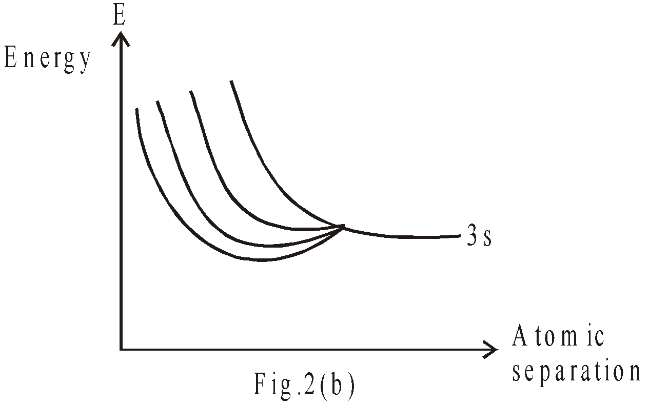
As we bring together a large number of atoms to form a solid, the same sort of effect occurs. When the sodium atoms are far apart, all 3s electrons have same energy & as we begin to move them together, the energy levels begin to “split”. The situation for four sodium atoms is shown in fig 2(b). As the number of atoms is increased (may be 1020 atoms), the levels become so numerous & so close that we can no longer distinguish the individual levels as shown in fig 2(c). We can regard the N atoms as forming an almost continuous band of energy. Since those levels were identified with 3s atomic levels of sodium, we refer to the 3s band.
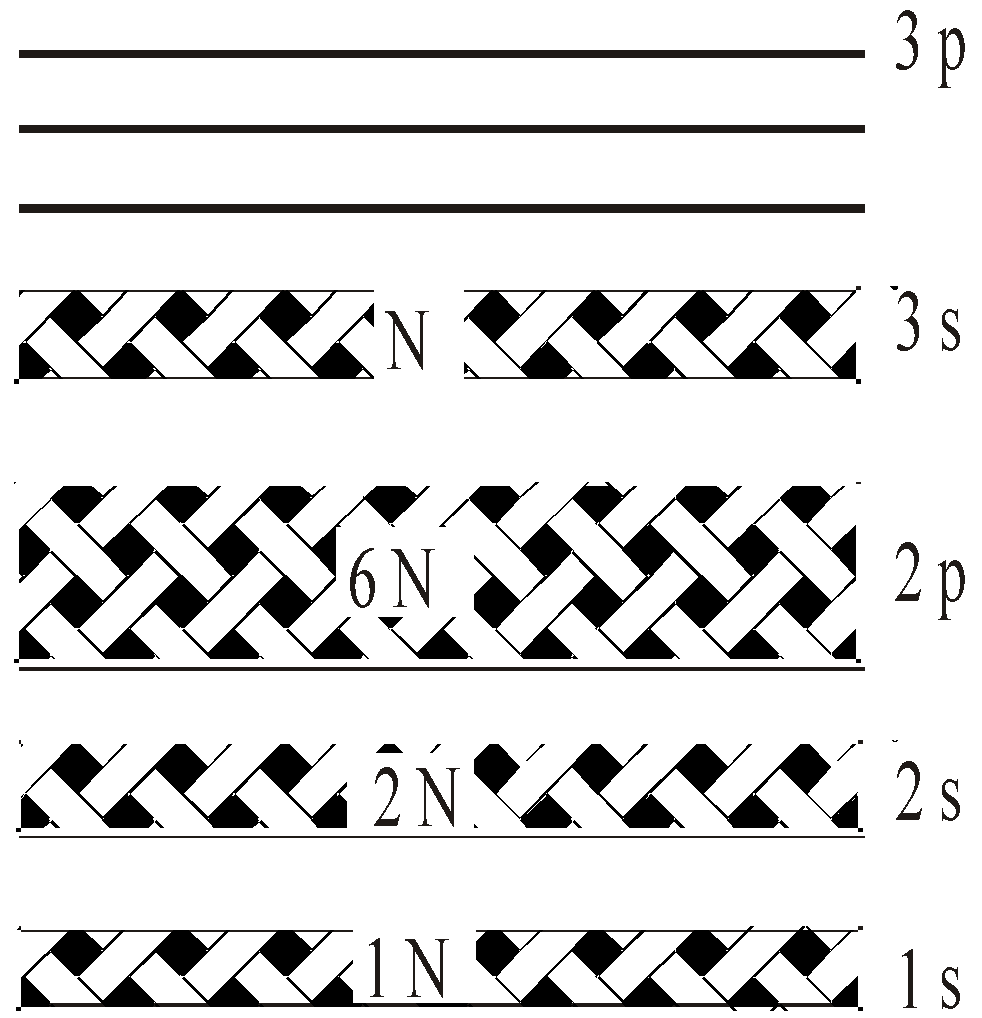
Fig. 3- Energy bands in sodium metal (G-state)
Each band has a total of N individual levels. Each level can hold 2 × (2 + 1) electrons ( is azimuthal quantum number), so the capacity of each band is 2(2 + 1)N electrons.
Fig – 3 shows a complete representation of energy bands in sodium metal. The 1s, 2s & 2p bands are each full, 3s band is half & 3p band is completely empty. The 1s & 2s bands each contain 2N electrons & 2p band contain 6N electrons. The 3s band contain N electron, so it is half filled. The band, which can hold 6N electrons is completely empty.
When we add energy to a system i.e., to sodium metal, the electron can move from filled state to empty state. In this case, the electron can move from partially full states of 3s band to empty states of 3s band by absorbing small amount of energy or move to 3p band by absorbing larger amount of energy.
In a solid at zero temperature, the electron settle into the available states of lowest energy. The lower energy bands will therefore be completely filled & the upper most energy band will be either completely filled or partially filled, depending on the number of electrons & on the number of available states. The difference between conductor & insulator arises from a partially filled or a completely filled uppermost energy band.
CONDUCTORS, INSULATORS AND SEMICONDUCTORS
CONDUCTORS
A conductor such as sodium, has a partially filled band (in sodium, the uppermost band 3s is half filled). In these substance, electrons are free to move by applying an electric field, because unoccupied states are available in uppermost band (in 3s band of sodium only half states are completely filled & half states are empty or unoccupied). Therefore these electrons are mobile & can contribute to electrical & thermal conductivity. For example the energy bands of sodium metal are shown in fig.4.
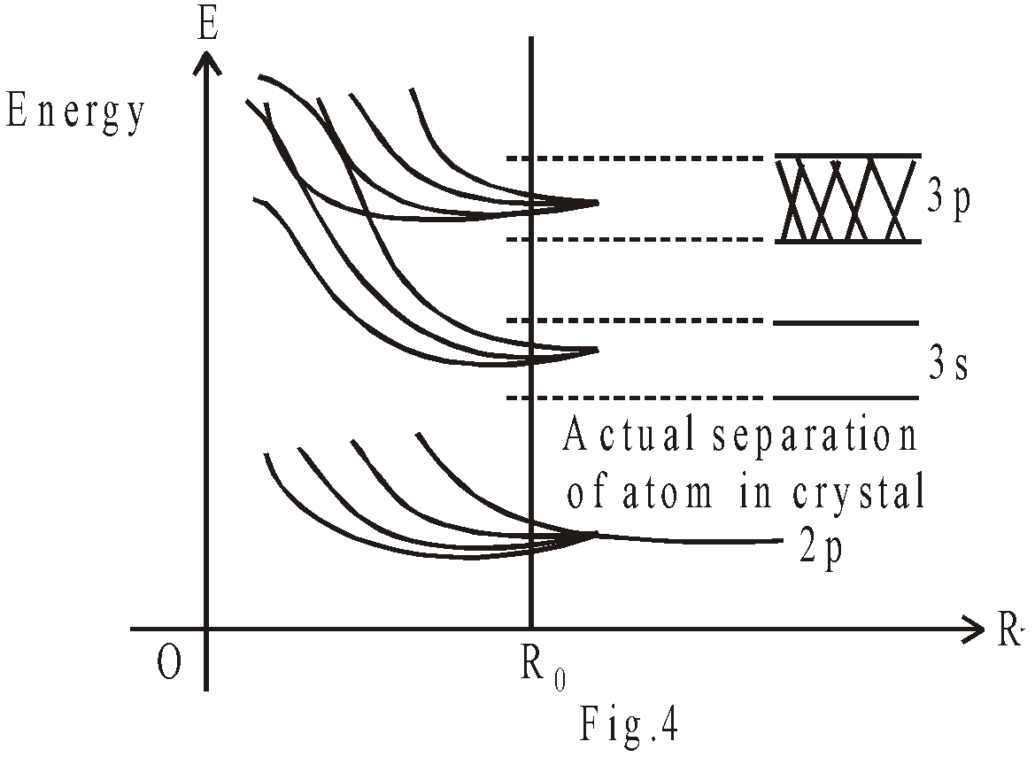
Origin of energy bands in sodium metals, as atoms move together the energy level spreads into bands.
In an isolated sodium atom, the six 3p lowest excited state for valence electrons are about 2.1 eV above two 3s G-states. But in solid sodium the 3s & 3p bands are spread out enough so that they actually overlap, forming a single band. Because each sodium atom has only one valence electron but eight 3s & 3p states, that single band is only 1/8 filled & other states are unoccupied.
INSULATORS
In these substances (such as diamond), the upper most level is completely filled i.e., no unoccupied state is available for electron to move. The nearest unoccupied states are in next band (called C.B.), but this is separated from filled band (called V.B.) by an energy gap (Eg) of about 6eV. Hence electron refuses to carry an electric current.
SEMICONDUCTORS
A semiconductor, has a completely filled valence band i.e., it resembles an insulator at zero temperature. However, the gap between this filled valence band & next band (C.B.) is small, about 1eV or less. Hence electrons can easily make the transitions from one band to another at room temperature & then carry an electric current (Silicon and germanium are semiconductors).
In a semiconductors, in thermal equilibrium, nenh = ni2
There are two types of semiconductor.
- Intrinsic (or pure) semiconductors : These semiconductors are pure materials in which the thermal vibrations of the lattice have liberated charge carriers (i.e., electrons & holes). In intrinsic semiconductor, the number of electrons (ne) are equal to the number of holes (nh).
- Extrinsic (or impure or doped) semiconductors : They are impure semiconductors in which minutes traces of impurity introduces mobile charge carriers [which may be +ive (holes) or -ive (electrons)] in addition to those liberated by thermal vibration.
Again there are two types of extrinsic semiconductors.
- N-type semiconductor : When we add a pentavalent impurity in intrinsic semiconductor, then we obtain N-type semiconductor. The pentavalent impurity substances are P, As & Sb. In N-type semiconductors, the electrons are majority carriers & holes are minority carriers.
i.e., ne >> nh
- P-type semiconductor : When we add a trivalent impurity in intrinsic semiconductor (such as B, Al, In), we obtain p-type semiconductor.
In p-type semiconductors, the holes are majority carriers & electrons are minority carriers.
i.e., nh >> ne
In acceptor impurity (trivalent element) energy level is just above the top of valence band (V.B.)
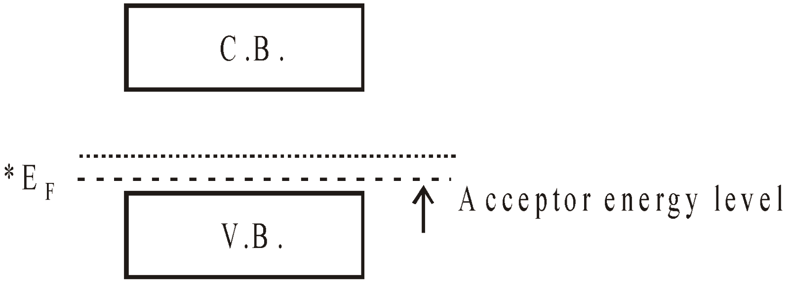
(*EF is called fermi level & at T = 0 all the states below are completely filled. In N-type semiconductor it lies between conduction band & donor energy level Ed & in case of P-type, it lies between acceptor level Ea & valence band. In intrinsic semiconductor the EF level lies in midway between C.B. & V.B.)
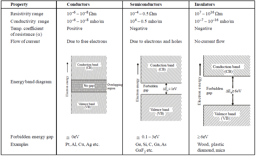
COMPARISON BETWEEN CONDUCTORS, SEMICONDUCTORS AND INSULATORS
COMMON DEFAULT
× Incorrect. N–type semiconductors are negatively and P–type semiconductors are positively charged.
√ Correct. Both N–type and P–type semiconductors are neutral because these are made up of neutral atoms.
× Incorrect. Mobility of holes is greater than mobility of electrons
√ Correct. Mobility of holes is less than mobility of electrons because mobility of holes takes place in valence band and mobility of electrons takes place in conduction band.
KEEP IN MEMORY
- Width of forbidden energy gap = Spacing between the top of valence band and the bottom of conduction band.
- At absolute zero temperature (0 K), there are no free electrons in the conduction band of a semiconductor.
- A good number of semiconductors (elemental and compound) have been discovered but the most frequently used are germanium (Ge) and silicon (Si) of group-IV of periodic table because the forbidden energy gap of them is small (of the order of 1 eV) so that at ordinary room temperature covalent bonds break easily and free electrons become available in the conduction band.
- Important compound semiconductors are gallium arsenide (GaAs), lead sulphide (Pbs), cadmium sulphide (Cds), indium phosphide (InP), etc.
- Holes doesn’t exist in conductors but only in semiconductors. They are deflected by electric and magnetic fields like electrons. Their movement contributes to electric current similar to electrons.
P-N JUNCTION DIODE
If we join a piece of n-type to a piece of p-type semiconductor by appropriate method, then we obtain p-n junction diode. The two ends of p-n junction is provided with metallic conductors for the application of an external voltage. It is clear that p-type has more holes concentration but less concentration of electrons than n-type semiconductor.
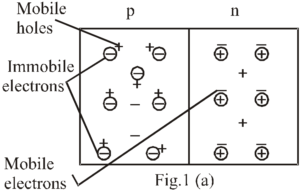
Due to this difference in concentration, density gradient is established across the junction resulting in majority carriers diffusion : Holes (+ive ions) diffuses from p-type to n-type & electrons (-ive ions) from n-type to p-type (shown in fig (a)) & terminating their existence by recombination.
DIFFUSION AND DRIFT CURRENT
DIFFUSION CURRENT
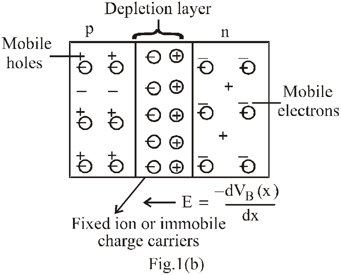
We know that due to concentration difference, holes diffuse from p-side to n-side (in figure -1(a)) they move from left to right) & electron diffuse from n-side to p-side (in fig 1(a) they move from right to left). But electric field at junction repels the holes as they come to depletion layer & only those holes which have high kinetic energy are able to cross the potential barrier. Similarly electric field at junction repels electrons & those having high kinetic energy cross the junction.
The electric potential of n-side is more +ive (or higher) than p-side –ive (or lower). The variation of potential barrier VB is shown in fig (c).
The potential difference created across the p-n junction due to the diffusion of electrons and holes is called potential barrier. So diffusion results in an electric current from p-side to n-side known as diffusion current.
DRIFT CURRENT
Due to thermal collision, sometimes a covalent bond is broken & electron-hole pair is created. But those electron-hole pairs are destroyed easily due to recombination. This process [generation of electron-hole (e-h) pair] occurs in the whole part of material.
But, if e-h pair is created in depletion region, the electron is quickly pushed by electric field towards n-side & holes towards p-side. As e-h pairs are continuously created in depletion region, there is a regular flow of electron towards n-side & holes towards p-side & so current flows from n-side to p-side. This current is drift current.
In steady state the magnitude of drift current is equal to diffusion current & since they are in opposite direction, hence there is no net transfer of charge at any cross section.
This recombination produces narrow region near junction called depletion layer. Since this region is depleted of free or mobile charge carrier and contains only immobile charge carriers, hence it is called depletion region. Due to these immobile charge carriers, a potential barrier VB is established & further diffusion is stopped & equilibrium is reached (shown by fig. 1(b)). The sign of VB is +ive towards the n-type & -ive towards p-type.
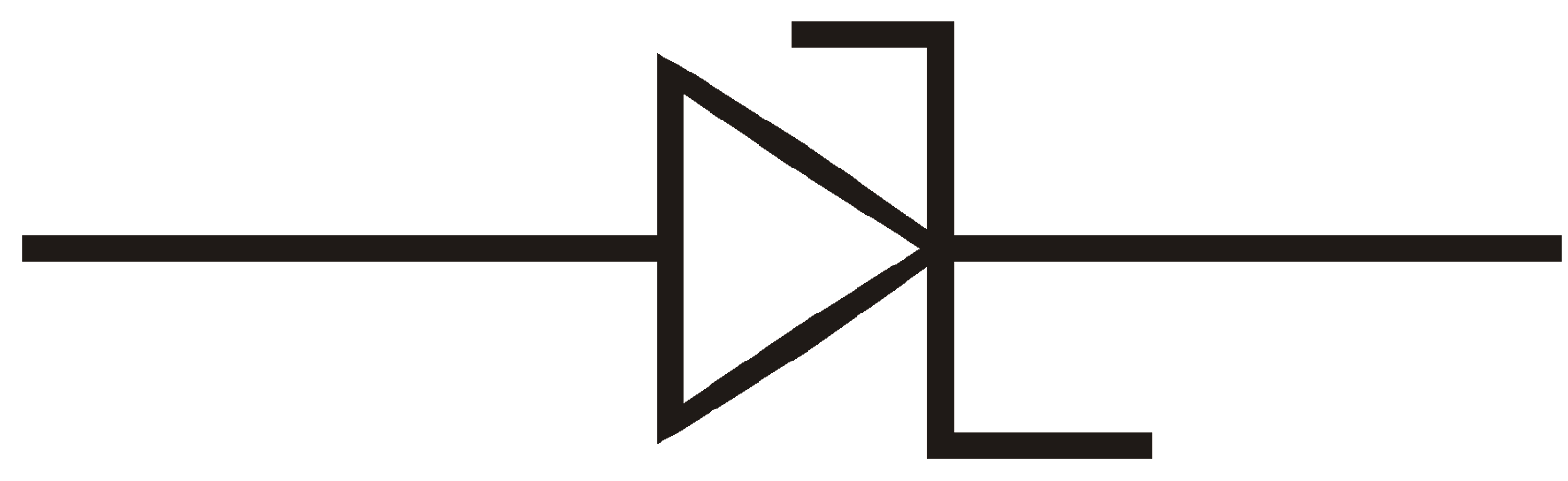
The schematic symbol of diode & corresponding equivalence in terms of VB are shown below in fig. 2 (a) & (b).
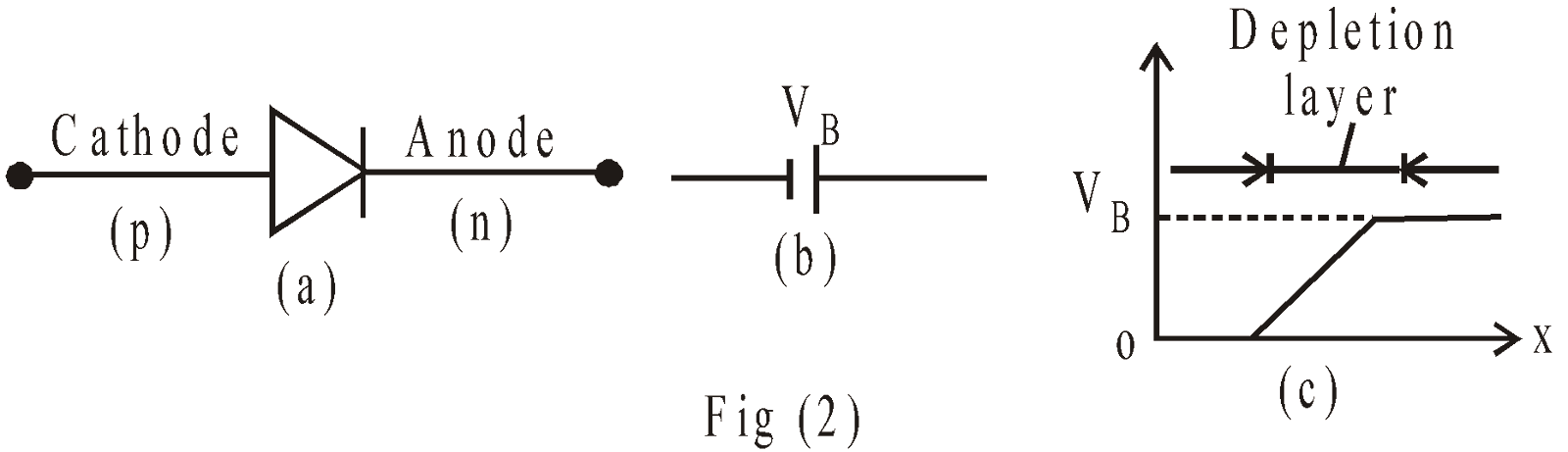
In fig-2(a) the triangle shows the direction of current.
For Si diode the value of VB is 0.7V
For Ge diode the value of VB is 0.3V
FORWARD AND REVERSE BIAS OF P-N JUNCTION DIODE
FORWARD BIAS
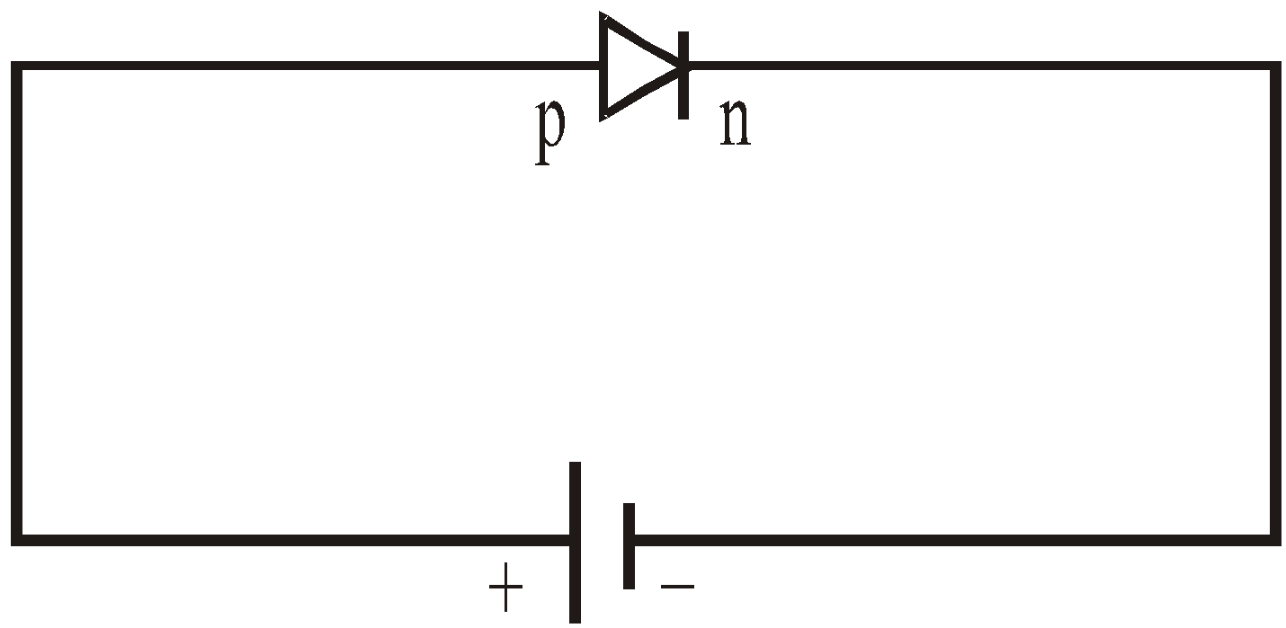
When p-side of the p-n junction is connected to the +ve terminal of a battery and n to –ve terminal, conduction takes place and the diode is said to be forward biased.
REVERSE BIAS
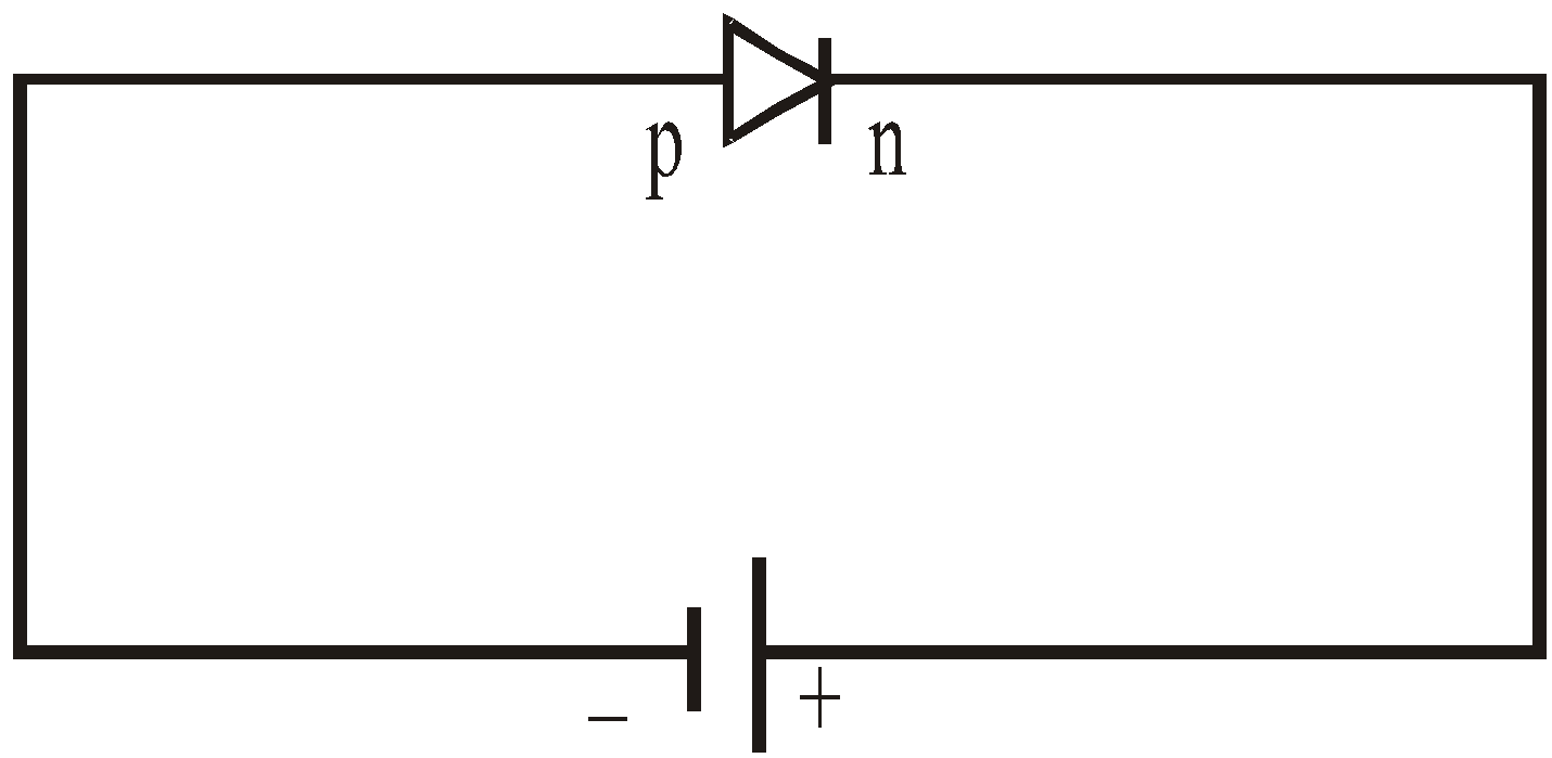
When p-side of the p-n junction is connected to the -ve terminal of a battery and n-side to the +ve terminal, there is no conduction takes place and diode is said to be reverse biased.
EFFECT OF BIASING
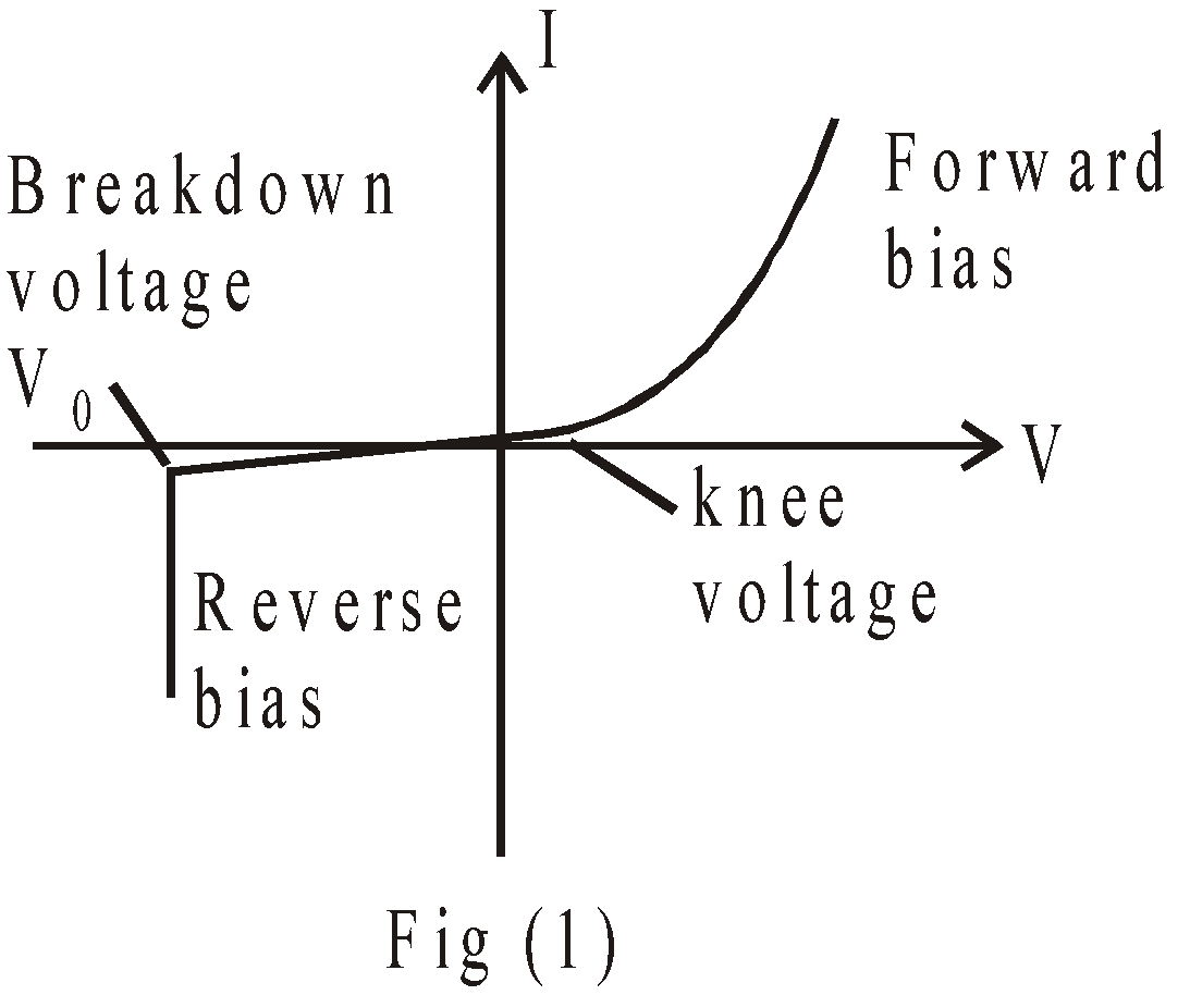
In forward bias, the thickness of depletion layer decreases and potential barrier reduces, while in reverse bias, the thickness of depletion layer increases and potential barrier also increases. In forward bias the current increases exponentially & in reverse bias, the current remains constant at very small magnitude upto breakdown voltage Vo & after that it increases sharply without any further increase of reverse voltage shown in fig.1.
V-I characteristics of a p-n junction diode in forward and reverse bias
The effect of forward biasing & reverse biasing on potential barrier are shown in fig.(2).
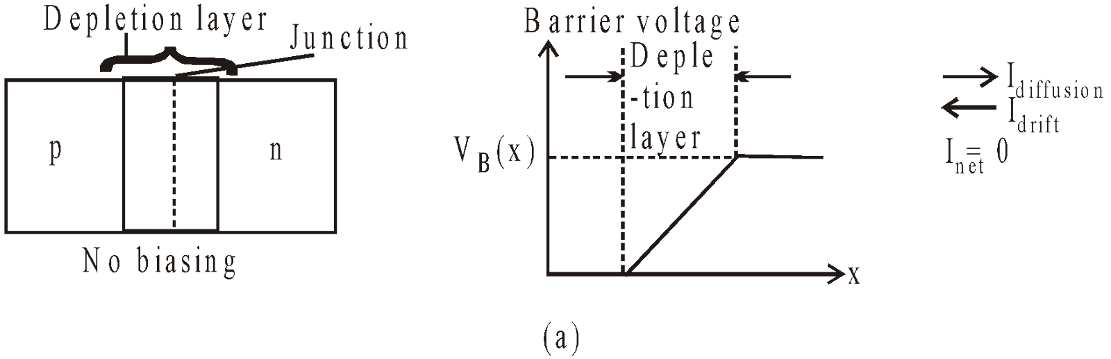
Fig.(2)(a) p-n junction without biasing
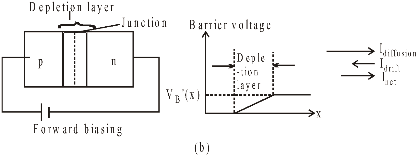
Fig.(2)(b) p-n junction with forward biasing
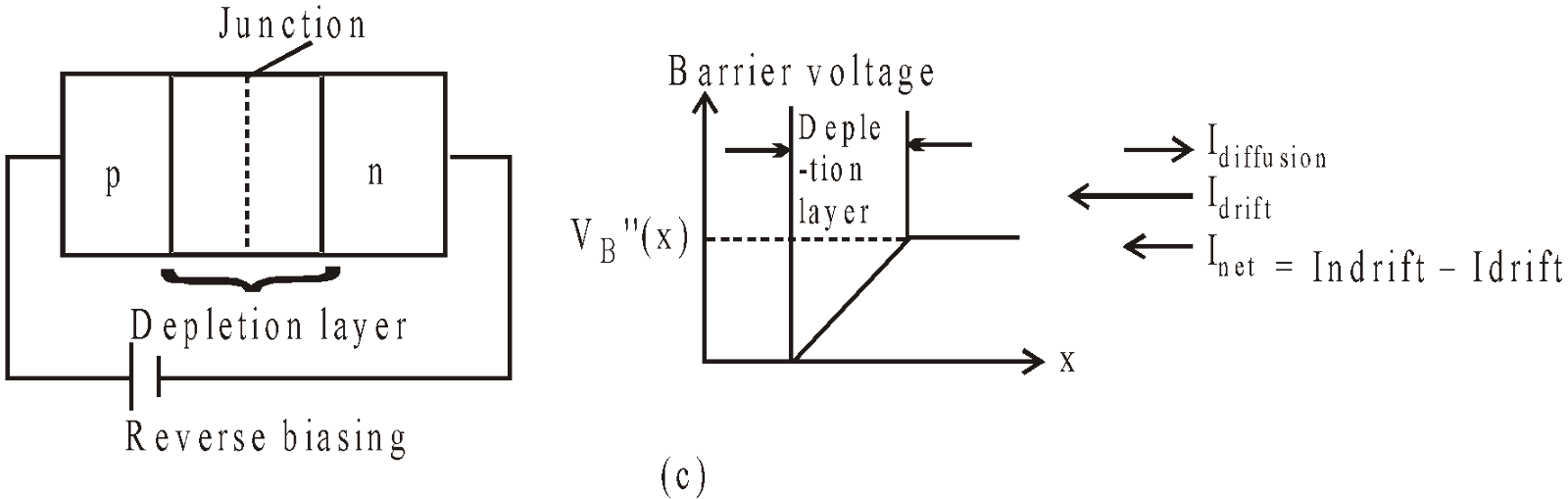
Fig.(2) (c) p-n junction with reverse biasing
In forward bias the expression of current is 
where V is applied voltage
Io is reverse saturation current
e is fundamental electronic charge
KB is Boltzmann constant and
T is temperature
KEEP IN MEMORY
- Width of depletion layer

- Depletion is directly proportional to temperature.
- Resistance is forward bias Rforward ≈ 10Ω – 25Ω and resistance in reverse bias Rreverse ≈ 105Ω.
- Under suitable reverse bias breakdown occurs and voltage gets stabilized at Zener voltage.
- Junction diode (p-n junction) can be used to convert the a.c. current to d.c. current i.e. as a rectifier. The process of conversion from a.c. to d.c. is called rectification.
- p-n junction diode can be used as a half wave or full wave rectifier. A device used to convert dc into ac is called inverter.
 Avalanche or zener diode or breakdown diode used in voltage stabilisation.
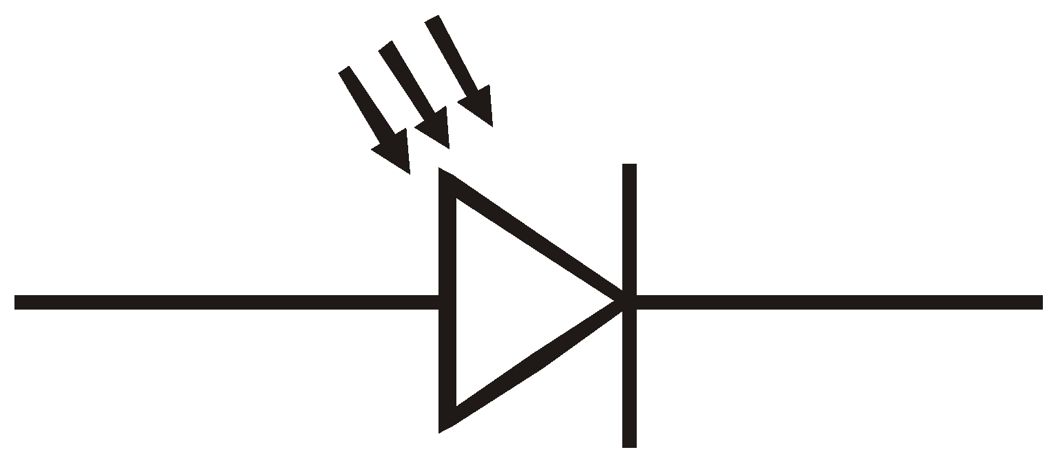 Photodiode, used in automatic switching of light, fire and burglar alarm
- A zener diode operating in the breakdown region is equivalent to a battery. This property of zener diode makes it suitable for voltage regulation (holding voltage constant).
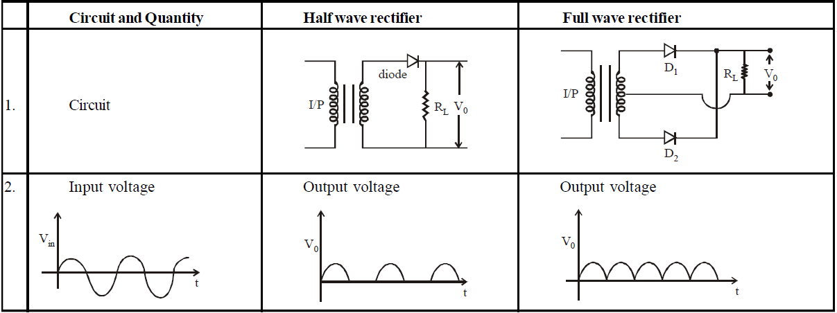
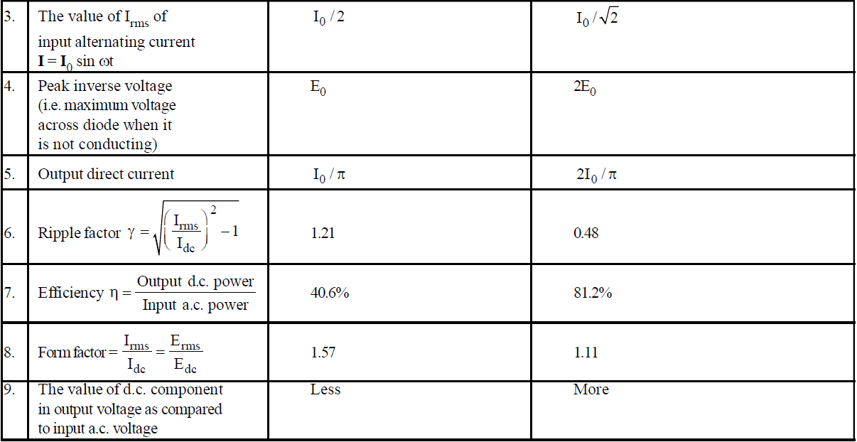
SOME IMPORTANT RESULTS OF HALF-WAVE AND FULL-WAVE RECTIFIER
TRANSISTOR
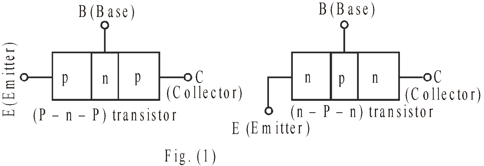
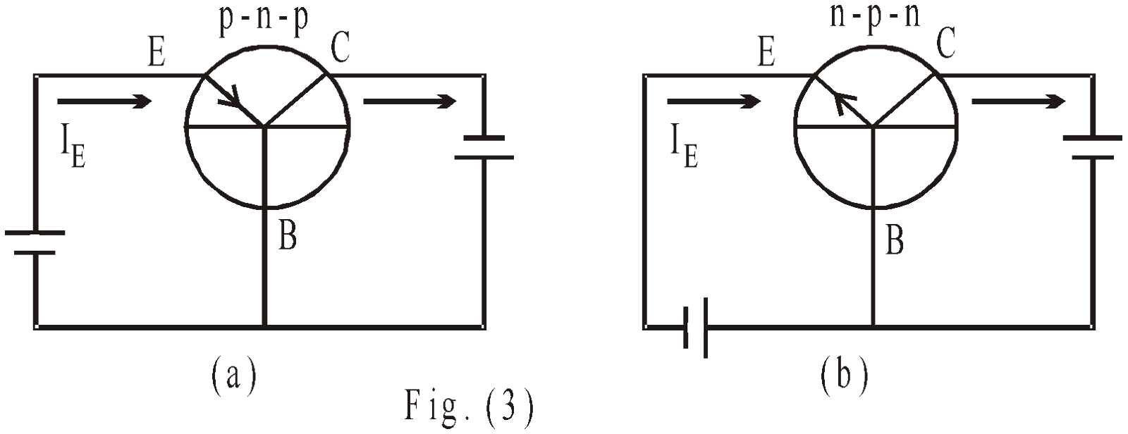
Transistors are three terminal (solid state) devices just like triode. It can be assumed to consist of two back to back p-n junctions. In practice a junction transistor (p-n-p) consists of silicon (or germanium) bar crystal in which a layer of n-type silicon (or Ge) is sandwiched between two layers of p-type silicon & we get p-n-p transistor. Alternatively it may consist of a layer of p-type between two layers of n-type material & we get a n-p-n transistor as shown by fig.(1).
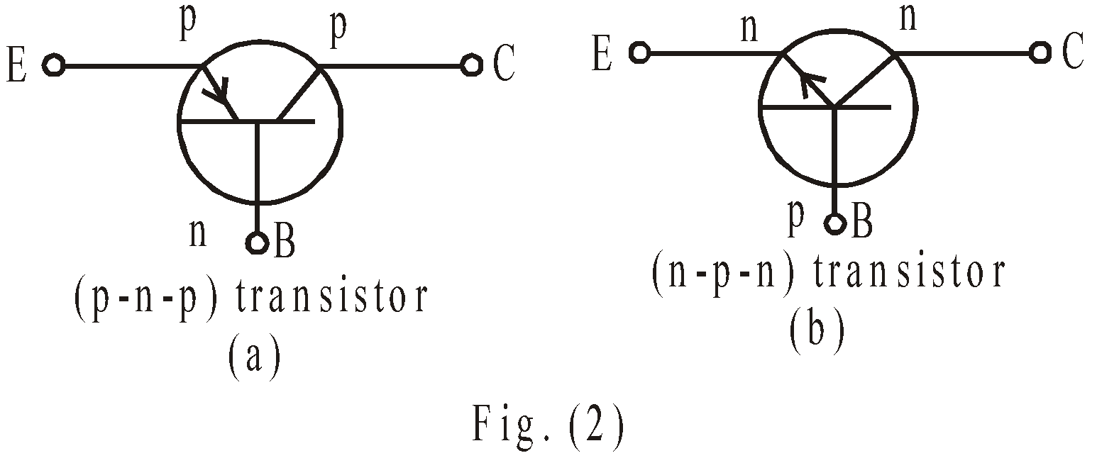
The schematic symbols of transistor are
COMPONENTS OF TRANSISTOR
- Emitter (E) : It supplies charge carriers (electron in n-p-n transistor and holes in p-n-p transistor) & it has high density of impurity concentration i.e., highly doped. It is always forward biased.
- Collector (C) : It is a region on other side of base. It has maximum area out of other sections (emitter & base) of transistor to dissipate the heat. It collects the charge carriers & it is always reverse biased.
- Base (B) : It is middle region which forms the two junctions between emitter & collector. It is very lightly doped.
BIASING OF TRANSISTOR
In proper biasing of transistor the input (i.e., base emitter junction) is always forward biased & output (i.e., collector base junction) is always reverse biased as shown in fig.(3)
This scheme of biasing is same for all three transistor configurations;
- Common base configuration (CB)
- Common emitter configuration (CE)
- Common collector configuration (CC)
WORKING OF TRANSISTOR
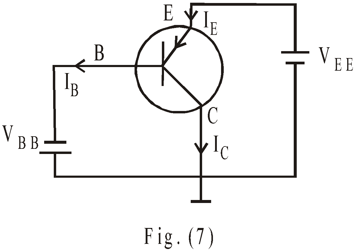
Fig. (4) shows a common base (C.B.) configuration of p-n-p transistor. The forward biasing of emitter junction lowers the emitter base potential barrier, whereas the reverse biasing of collector junction increases the collector-base potential barrier. Hence holes (majority carriers in p-type) flows through emitter to base & constitutes an emitter current IE. Since emitter is heavily doped in comparison to base, so approximately (only 5% holes recombine with electrons in base region & constitute base current IB) 95% holes reach to collector & constitute collector current IC.
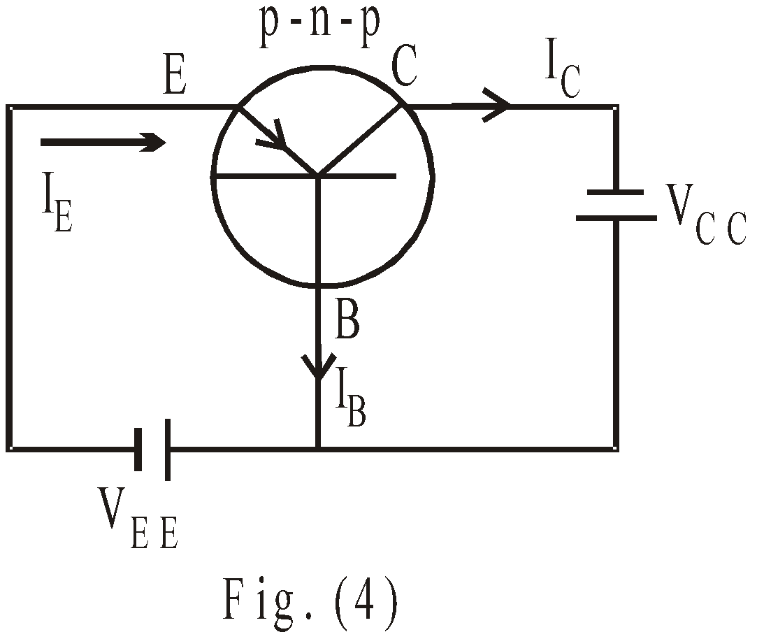
From Kirchhoff’s current law,
IE = IC + IB …(1)
Eq. (1) holds true regardless of circuit configuration or transistor type (p-n-p or n-p-n) that is used.
The current gain (B) of transistor is defined as ratio of collector current IC to base current IB
i.e.,  …(2)
…(2)
The value of β lies between 10 and 100. Since 
Current gain (α) is defined as the ratio of collector current IC to emitter current IE. The value of α is always less than unity.
Relation between α and β
CONFIGURATIONS OF TRANSISTOR
There are three types of transistor configuration. We can take either terminal as input terminal and other terminal as output.
- Common base configuration (CB)
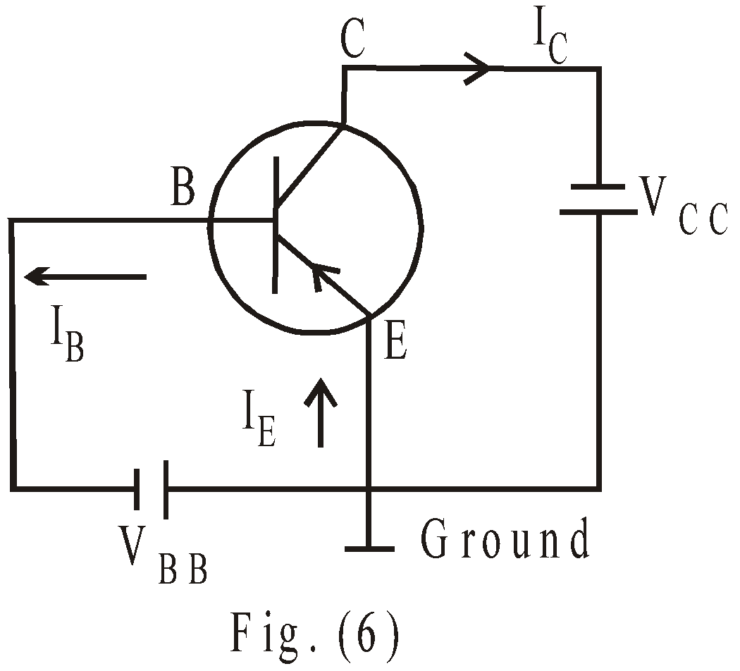
Here base terminal is common to both input & output terminals as shown in fig. (5). The emitter terminal is taken as input.
- Common emitter configuration (CE)
Here emitter terminal is common to both input and output terminals as shown in fig. (6). The base terminal is taken as input and collector is taken as output.
- Common collector configuration (CC)
Here the collector terminal is common to both input as well as output terminals as shown in fig. (7). The base terminal is input & emitter is output terminal.
TRANSISTOR AS AN AMPLIFIER
Amplification is the process of linearly increasing the amplitude of a signal. It is one of the major properties of a transistor. This amplifying action was produced by transferring a current from a low (base emitter loop is forward biased & hence provide low resistance path and collector base junction is reverse biased & hence gives high resistance path in common emitter configuration) to a high resistance circuit.
Common- Emitter (CE) Amplifier : Fig. 8 shows a basic common-emitter amplifier circuit in which we connect a signal source Vs. The input voltage loop is Vs, then from base to emitter through transistor to ground (common reference point) & then through VBE back to Vs. The output voltage loop consists ground, then from emitter to collector through RC. The emitter is connected to ground. During a +ive half cycle of Vs, the forward bias across the emitter base junction will be increased, while during –ive half cycle of Vs (signal source), the forward bias across emitter base junction will be decreased. Hence more electrons flow during +ive half cycle and so we obtain more collector current and so large voltage drop across RC and less value and VCE. In negative half cycle collector current decreases.
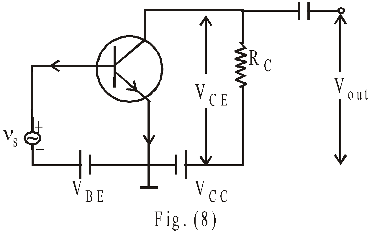
In the absence of input signal vs, a D.C collector current IC flows in collector circuit due to forward biased battery VBE. This is called zero signal collector current. So total collector current is

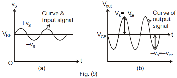
(a) Input signal superimposed on VBE
(b) Output amplifying signal wave from superimposed on VCE
The voltage from the collector to ground determines the output signal. When IC (during +ive half cycle) increases, VCE decreases & when IC decreases (during – ive half cycle) VCE increase. So output voltage is 180º out of phase with input signal in CE amplifier:
The current gain Ai is defined as,
The voltage gain Av is defined as,
The power gain Ap is defined as, Ap = Ai × Av
For example : Let VBE =0 .7V, VCC = 20V
IB = 60μA, IC = 3m A, RC = 3 kΩ
Then 
The collector current flowing through RC results in voltage drop:
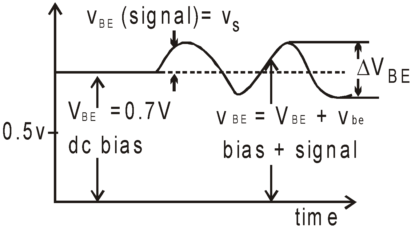
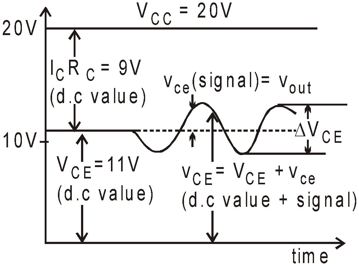
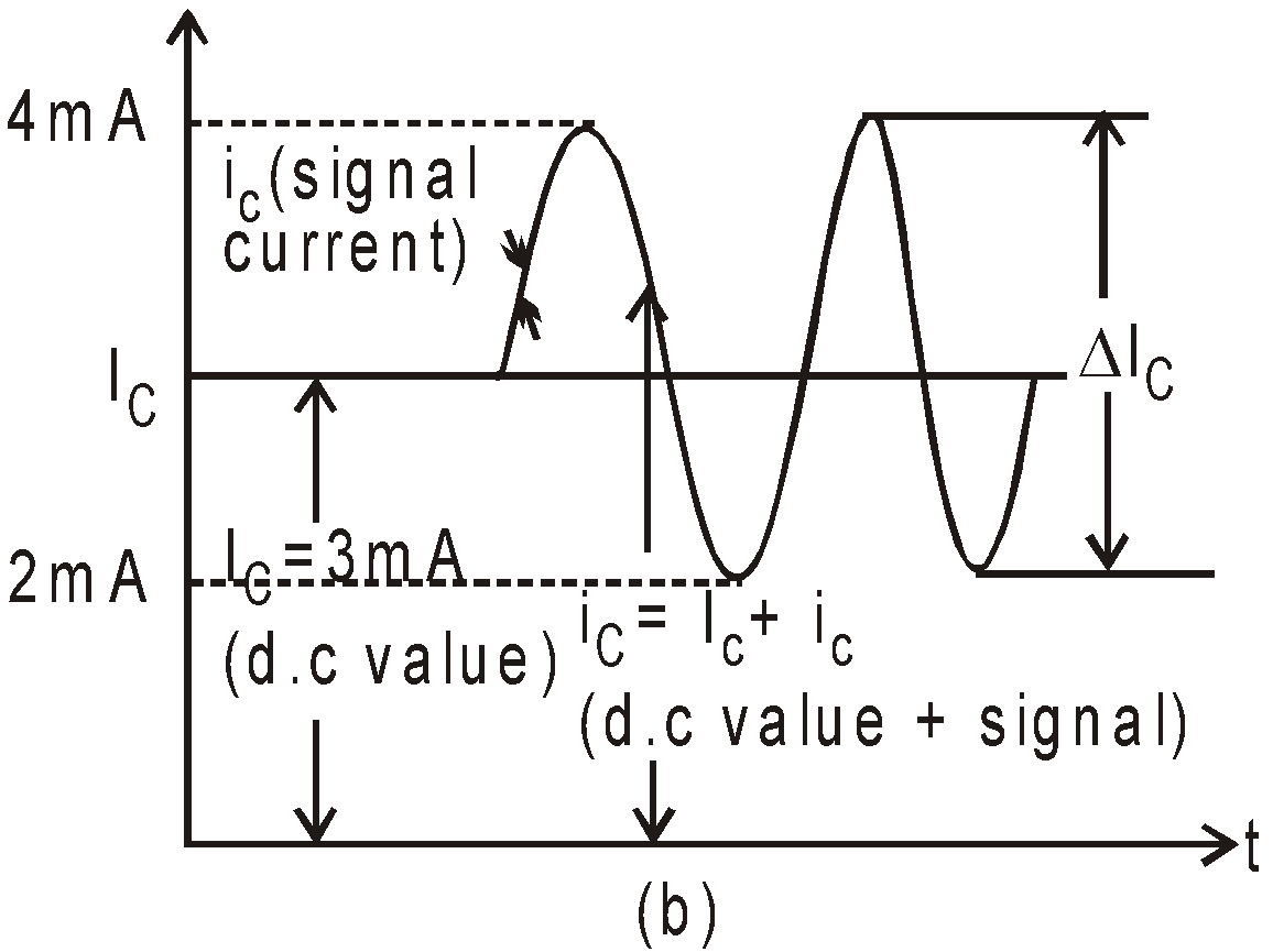
Fig. (a) Base waveforms or input waveforms (b) Collector waveforms or output waveforms.
ICRC = .003A × 3000Ω = 9.0V
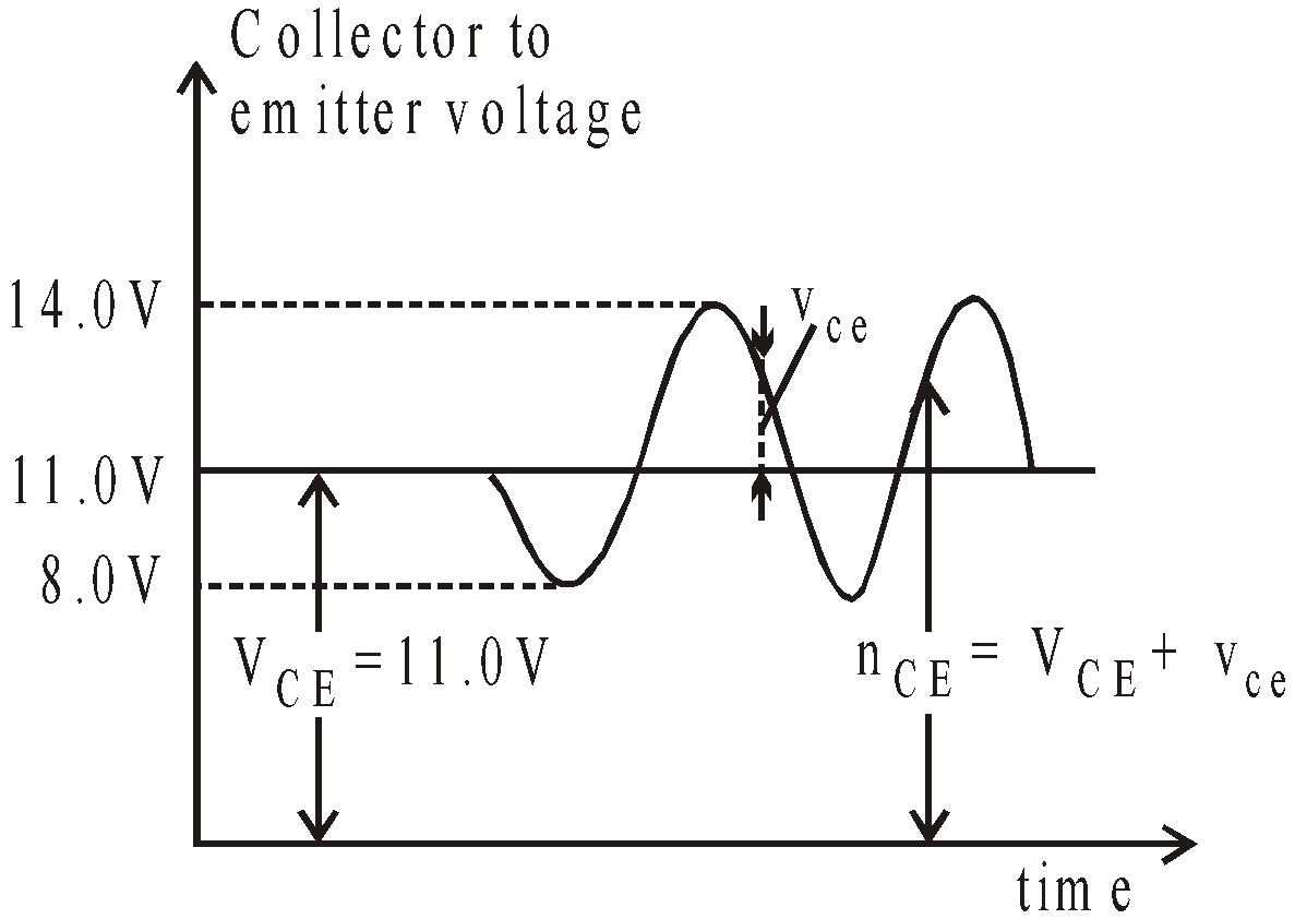
So by K.V.L the voltage from collector to emitter is
VCE = VCC – ICRC = 20 – 9 = 11.0V
Now we introduce signal voltage vs, which has peak value 50mV.
During +ive half cycle of vs = + 50mV, IB rises to 80μA & during –ive half cycle of vs = – 50mV. IB decreases to 40μA.
So change in base current is ΔIB (80 – 60) μA = 20μA
and change in collector current is ΔIC (βac ΔIB) = 50 × 20 = 1mA
It means during +ive half cycle IC becomes 4mA hence
VCE = VCC – ICRC = 20 – 12 = 8.V
During the negative half cycle IC becomes 2mA, hence
VCE = 20 – 6 = 14V.
so ΔVCE = 3V
so 
and Ap = Ai × Av = 3000
KEEP IN MEMORY
- Amplifier is a device used to increase the amplitude of input signal.
- Amplification factor of triode valve μ = gm × Rp where
gm = mutual or trans conductance and Rp = plate resistance. - Transistor is also used as an oscillator.
Frequency of transistor LC oscillator is given by ,
,
- In phase shift oscillator (which consists of three RC section), the frequency is given by

- Oscillator gives continuous, undamped oscillating output.
- Inverter : An oscillator which converts d.c. into a.c.
- An amplifier with feedback in proper phase and magnitude behaves as an oscillator.
- Barkhausen criteria : for amplifier to act as oscillator :
Gain with feedback, A’ = A/[1 – KA], K = feedback ratio.
Criteria to become oscillator, (1 – KA) = 0 where A’ is called closed loop gain & A is called open loop gain.
Criteria to become oscillator, (1 – KA) = 0 where A’ is called closed loop gain & A is called open loop gain.
- The basic rules for normal operation of a transistor are
- emitter-base junction is forward biased to offer a low resistance to the flow of current.
- collector-base junction is reverse biased to offer a high resistance to the flow of current.
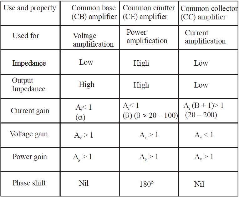
COMPARATIVE STUDY OF CB, CE AND CC AMPLIFIER
LOGIC GATES
A logic gate is a digital circuit that follow certain logical relationship between input and output voltages. They control the flow of information.
Basic logic gates : AND, OR and NOT gates.
AND GATE
The output is high or 1 when all inputs are high.
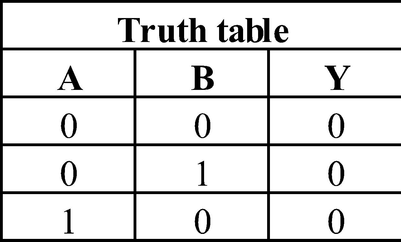
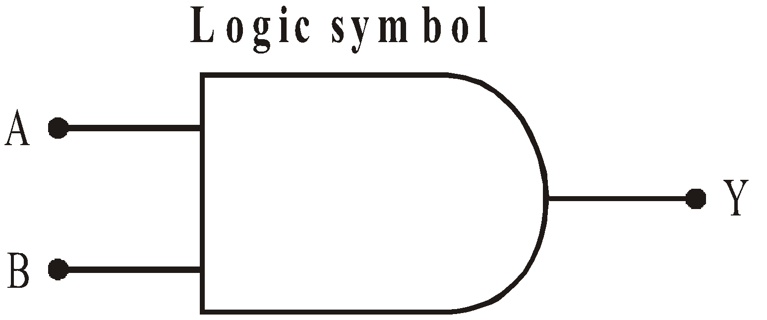
Boolean expression : A . B = y
OR GATE
Output is high even if one of the inputs is high.
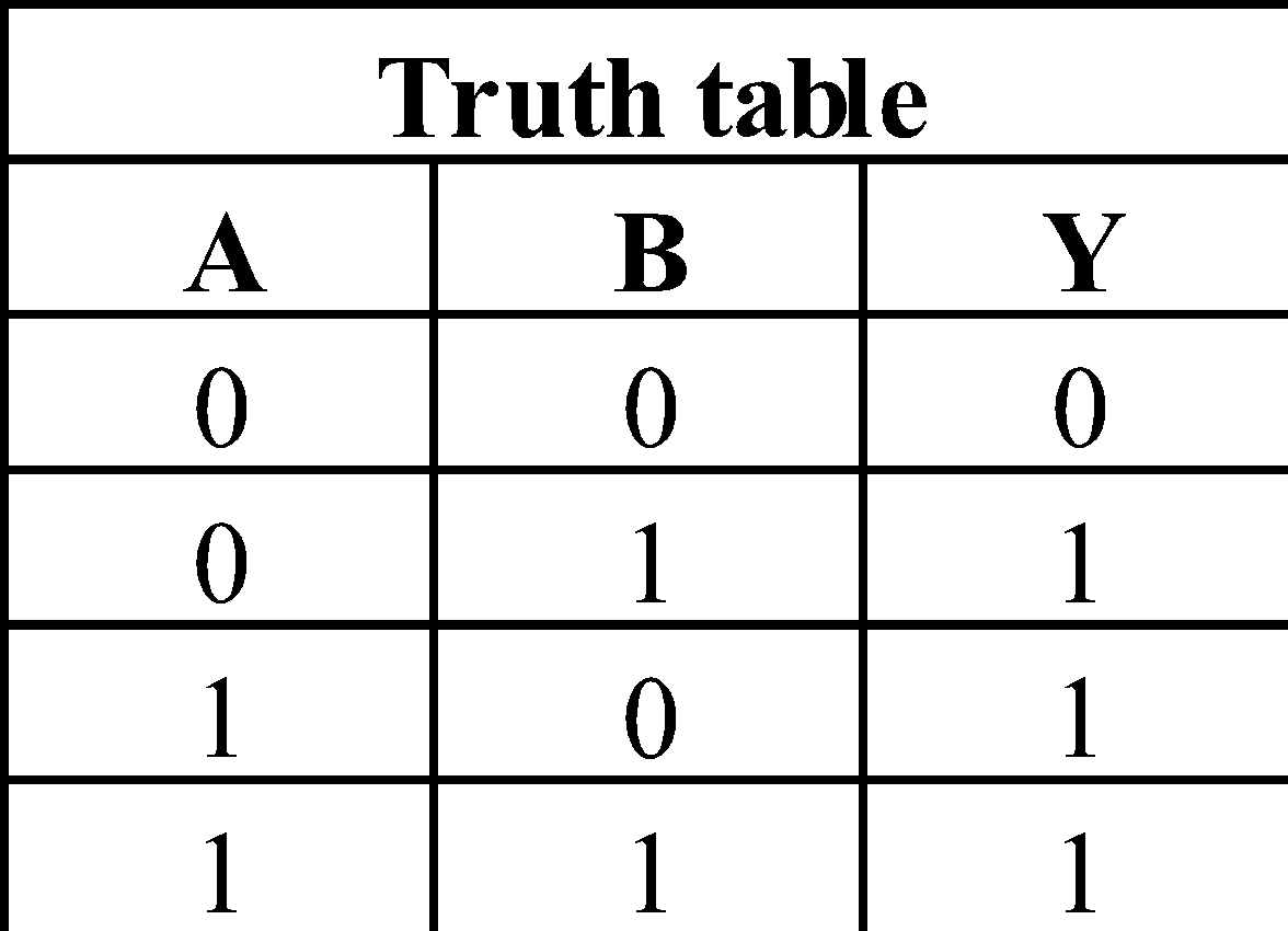
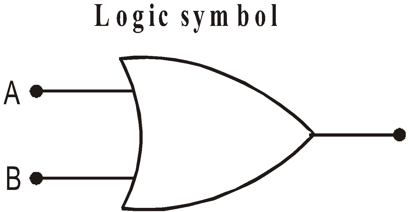
Boolean expression : A + B = y
NOT GATE
Output is not the input.
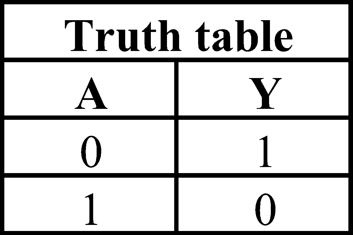
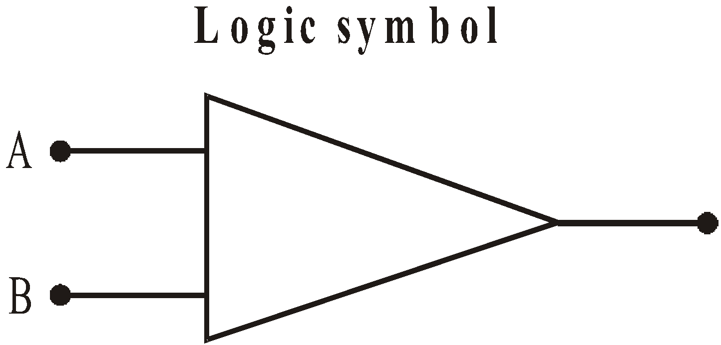
Boolean expression : 
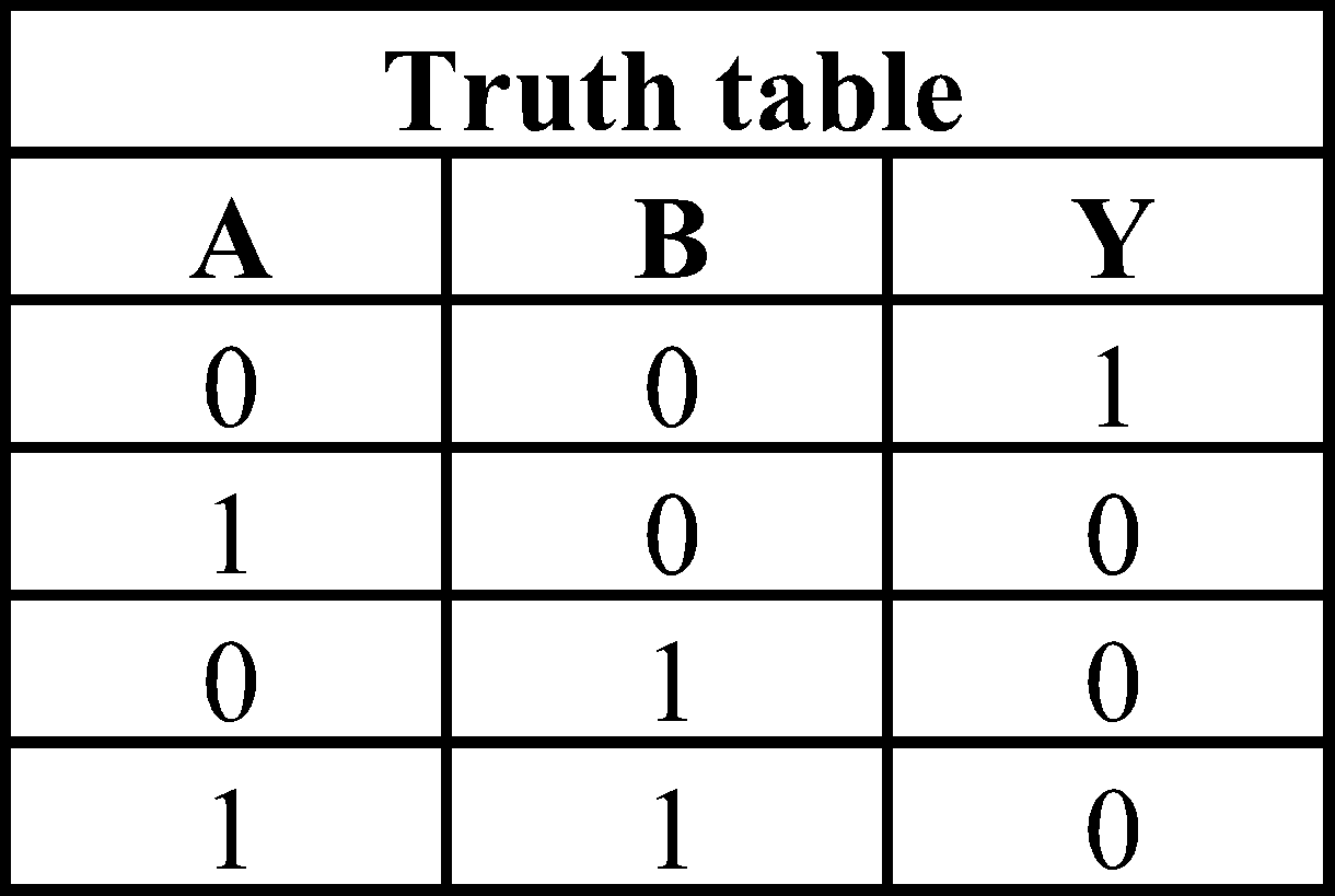
NAND GATE
It is the combination of AND and NOT gate. The output is high, even if all inputs are low (i.e., 0) or one input is low.
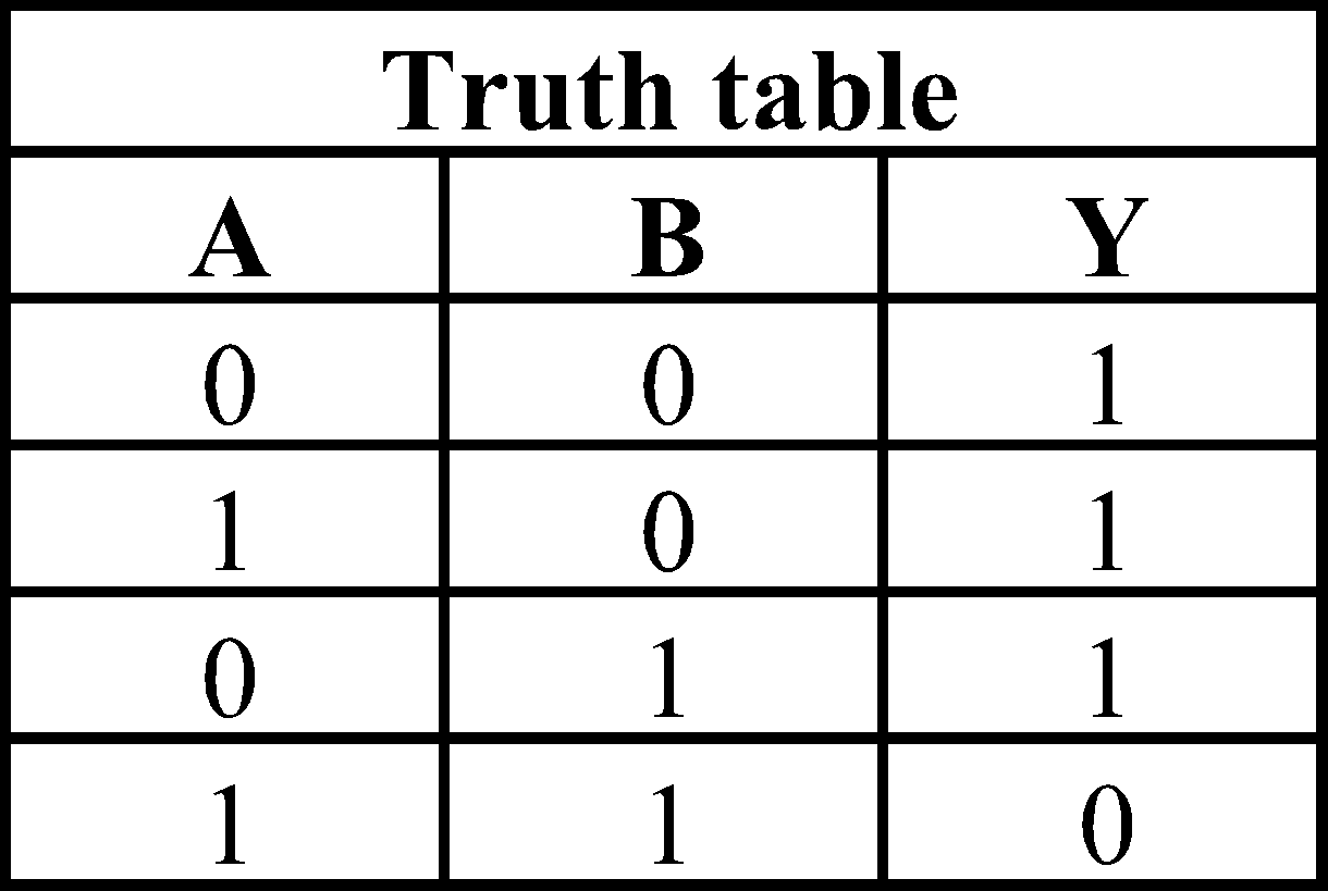
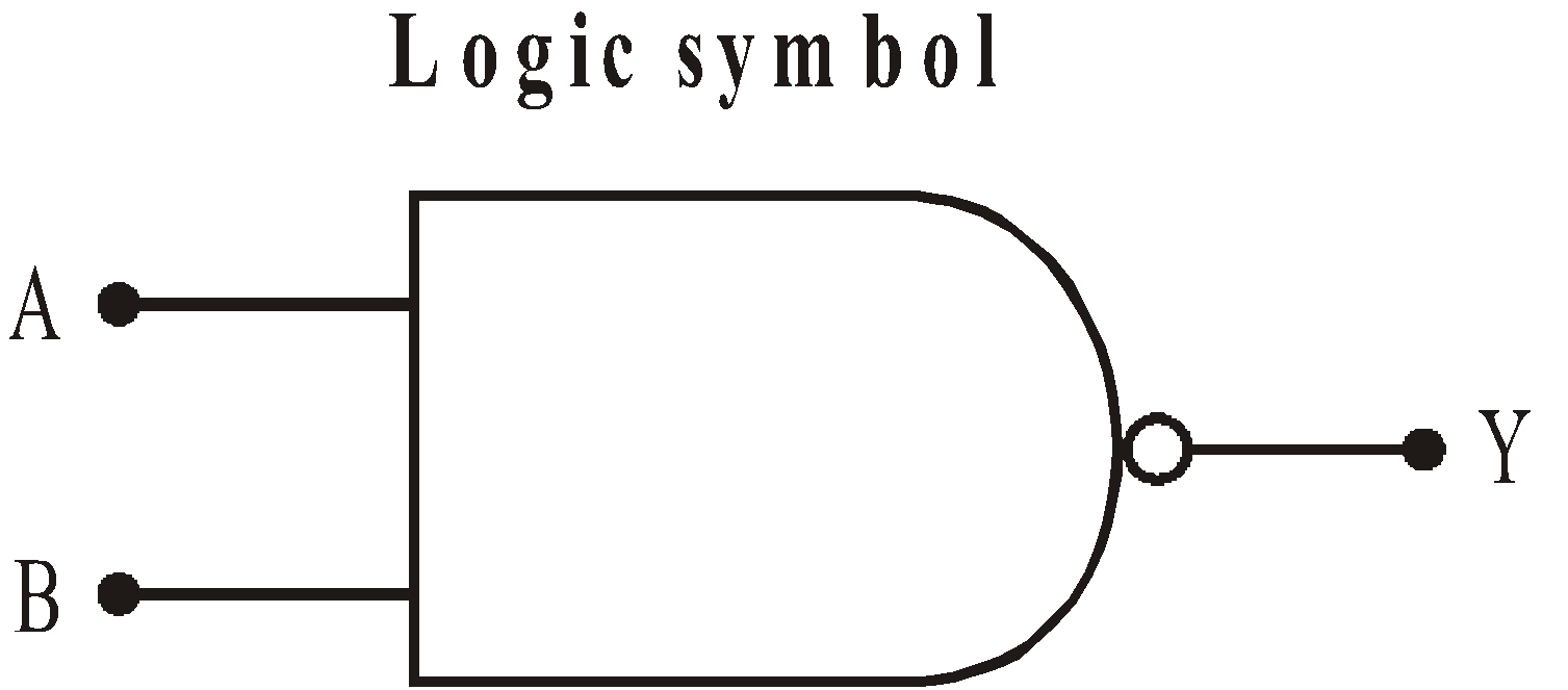
Boolean expression : 
NAND gate is called the building block of all digital circuits.
NOR GATE
It is the combination of NOT and OR gate. The output is high, when all inputs are low.
Boolean expression : 
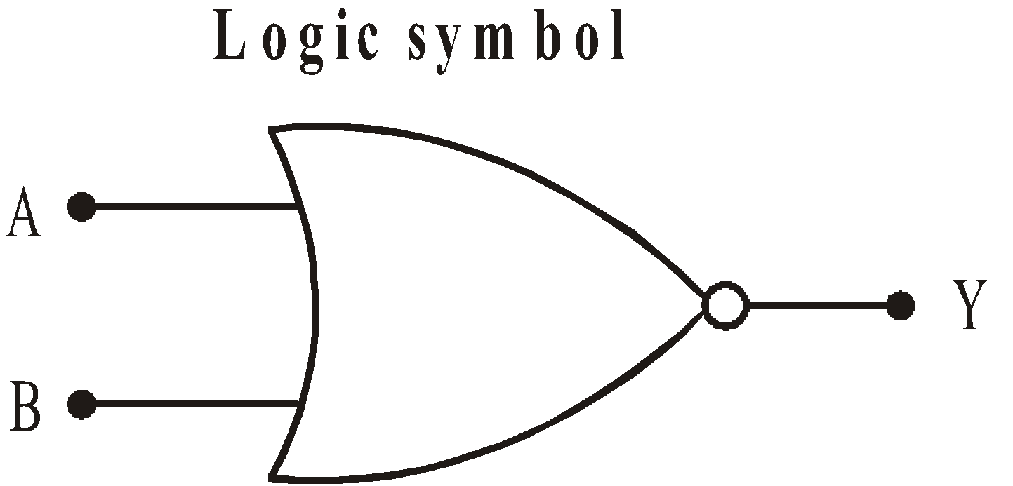
EXCLUSIVE OR (XOR) GATE
The output of a two input exclusive OR gate is at logical 1 if one and only one input accepts logical 0 (zero)
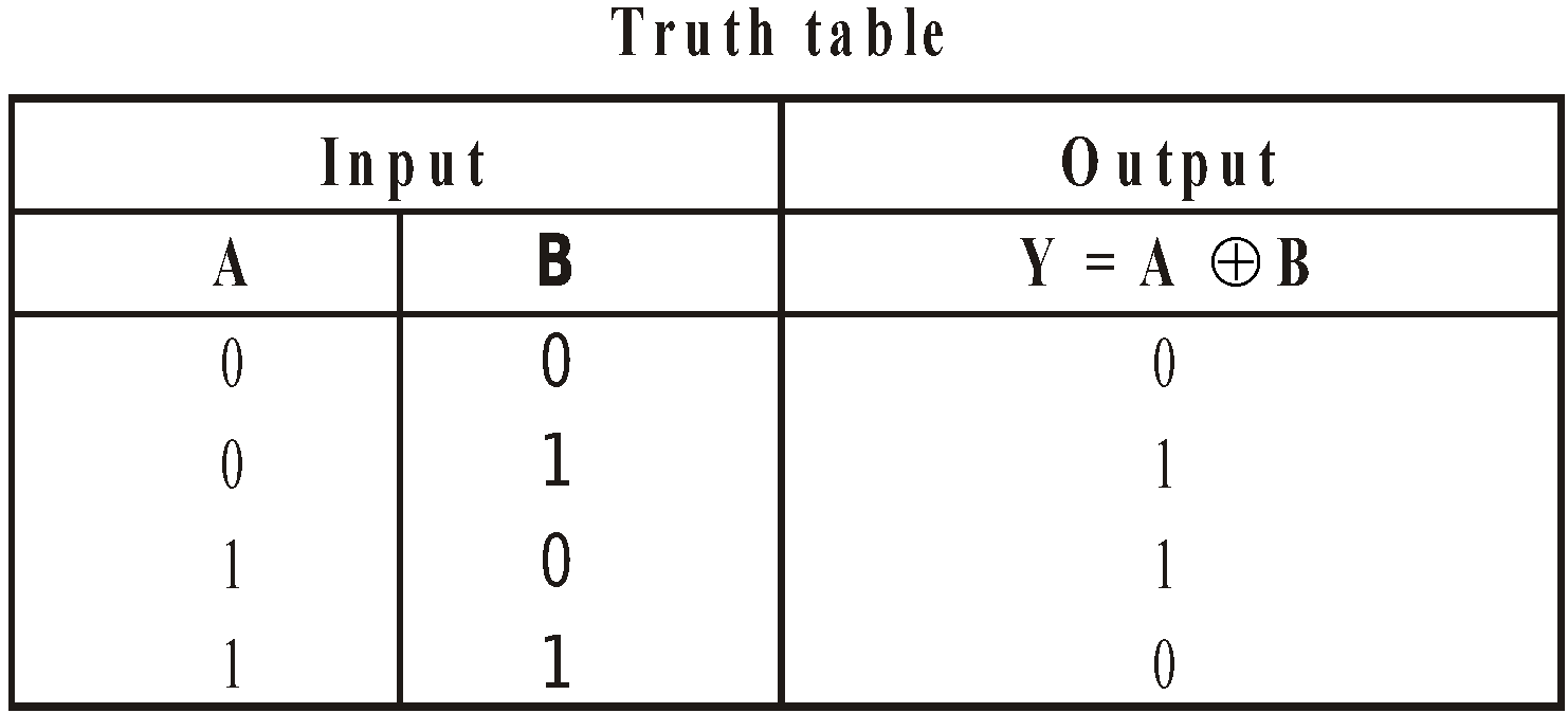
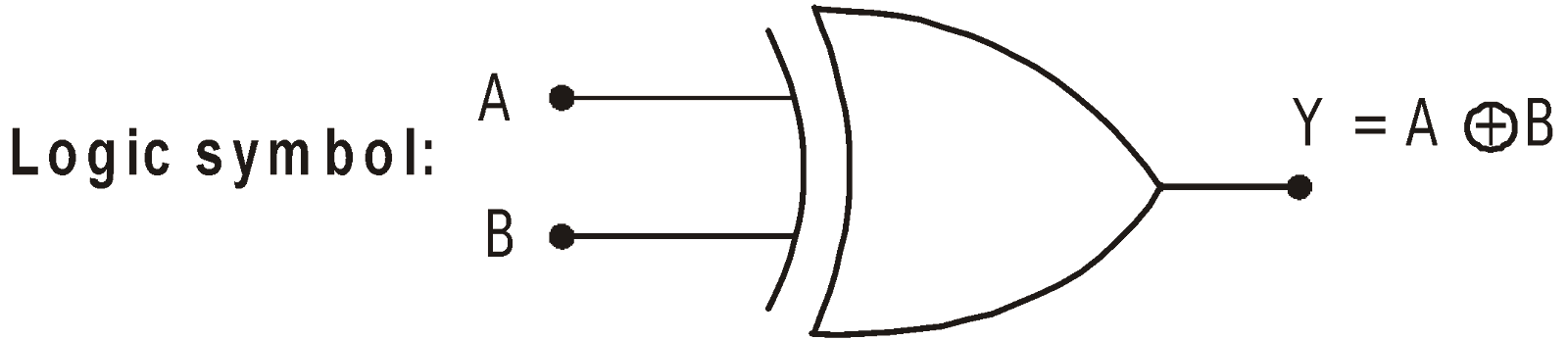
Logic expression : 
Note : This circuit is also called inequality comparator or detector because it produces an output only when the two inputs are different.
BINARY NUMBERS AND DECIMAL NUMBERS
- In a binary system, a number is expressed by only two digits 0 and 1. The base of the binary system is thus 2.
- 0 and 1 represent the coefficients of powers of 2.
- A binary digit (0 or 1) is known as a bit.
- A group of 4 bit is called a nibble & a group of 8 bit is called byte.
DECIMAL TO BINARY CONVERSION
- When the decimal number is an integer
Divide the decimal number progressively by 2 until the quotient is zero. The remainders of the successive divisions, written in the reverse order, give the binary number.
For example : We want to convert (9)10 into binary system.
 ( ↑ Read up)
So (9)10 = (1001)2
- When the decimal number is a fraction
The number is multiplied repeatedly by 2, and the carry in the integer position is recorded each time. The process is continued until the fractional part is zero or sufficient binary bits have been obtained.
Let we want to convert (0.85)10 into binary no. then
0.85 × 2 = 1.7 = 0.7 with a carry 1
0.7 × 2 = 1.4 = 0.4 with a carry 1
0.4 × 2 = 0.8 = 0.8 with a carry 0 (↓ Read down)
0.8 × 2 = 1.6 = 0.6 with a carry 1
0.6 × 2 = 1.2 =0 .2 with a carry 1
0.2 × 2 = 0.4 = 0.4 with a carry 0
So (0.85)10 = (0.110110)2
BINARY TO DECIMAL CONVERSION
- When the binary number is an integer
Binary can be converted into its decimal equivalent by noting that the successive digits from the extreme right of a binary number are the coefficients of ascending power of 2, beginning with the zeroth power of 2 at the extreme right.
- When the binary number is a fraction
The decimal equivalent of the binary number is found by multiplying each digit in fraction successively by
2–1, 2–2, 2–3…etc.
2–1, 2–2, 2–3…etc.
Let we want to convert (101.011)2 into its decimal equivalent. Then
(101.011)2 = 1 × 22 + 0 × 21 + 1 × 20 + 0 × 2–1 + 1 × 2–2 + 1 × 2–3 = (5.375)10
5.375 = 5 × 100 + 3 × 10⁻¹ + 7 × 10⁻² + 5 × 10⁻³
DEMORGAN THEOREMS
(i)  (ii)
(ii) 
These theorems are self-proved.
SOME BASIC BOOLEAN IDENTITIES
These above theorems, identities & relations can be easily proved.
KEEP IN MEMORY
- The basic concept of digital circuit has been provided by George Boole.
- Claude Shannon established an analogy between function of mechanical switches and Boolean algebra.
- Series combination of switches is equivalent to AND logic operation.
- Parallel combination of switches is equivalent to OR logic operation.
- NOT logic operation is performed on a single variable. That’s why it is called unary operation.
- AND, OR and NOT logic operations follow closure property, i.e., input as well as output are in either of the binary states.
- NAND and NOR gates are universal gates
- If the logic gate is changed from positive to negative or vice-versa; AND changes into OR, OR changes into AND, NAND changes into NOR and NOR charges into NAND.