Semiconductor Electronics: Materials, Devices and Simple Circuits Class 12 Physics MCQs
Question 1. In the given figure V0 is the potential barrier across a p-n junction, when no battery is connected across the junction. [NCERT Exemplar]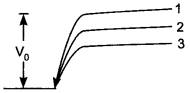
(a) 1 and 3 both correspond to forward bias of junction.
(b) 3 corresponds to forward bias of junction and 1 corresponds to reverse bias of junction.
(c) 1 corresponds to forward bias and 3 corresponds to reverse bias of junction.
(d) 3 and 1 both correspond to reverse bias of junction.
Answer/Explanation
Answer: b
Explanation:
(b) Height of potential barrier is decreases when p-n junction is forward bias.
Physics MCQs Pdf Question 2. In figure given, assuming the diodes to be ideal [NCERT Exemplar]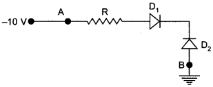
(a) D1 is forward biased and D2 is reverse biased and hence current flows from A to B.
(b) D2 is forward biased and D1 is reverse biased and hence no current flows from B to A and vice versa.
(c) D1 and D2 are both forward biased and hence current flows from A to B.
(d) D1 and D2 are both reverse biased and hence no current flows from A to B and vice versa.
Answer/Explanation
Answer: b
Explaination:
(b) Explanation:
10 V is the lower voltage in the circuit. Now p side of the p-n junction diode D1 is connected to lower voltage and n- side of D1 to higher voltage , thus D1, is reverse biased. In D2 p-side of p-n junction diode is at higher potential and n-side is at lower potential, therefore D2 is forward biased. Hence current flows through junction from B to A.
3. The output of the given circuit in figure is given below. [NCERT Exemplar]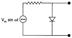
(a) would be zero at all times.
(b) would be like a half-wave rectifier with positive cycles in output.
(c) would be like a half-wave rectifier with negative cycles in output.
(d) would be like that of a full-wave rectifier.
Answer/Explanation
Answer: c
Explaination:
(c) Explanation:
When the diode is forward biased, the resistance of pn junction diode will be low then current in the circuit is maximum. In this situation, a maximum potential difference will appear across resistance connected in a series of circuit. This result into zero
Semiconductor Numericals Class 12 Question 4. Electrical conductivity of a semiconductor
(a) decreases with the rise in its temperature.
(b) increases with the rise in its temperature.
(c) does not change with the rise in its temperature.
(d) first increases and then decreases with the rise in its temperature
Answer/Explanation
Answer:
Explaination:
(b) With temperature rise, the conductivity of semiconductor increases.
5. The forbidden energy band gap in conductors, semiconductors and insulators are EG1,EG2 and EG3 respectively. The relation among them is
(a) EG1 = EG2 = EG3
(b) EG1 < EG2 < EG3
(c) EG1 > EG2 > EG3
(d) EG1 < EG2 > EG3
Answer/Explanation
Answer:
Explaination:
(b) In insulators, the forbidden energy gap is very large, in case of semiconductor it is moderate and in conductors the energy . gap is zero.
MCQ Physics Class 12 Question 6. In an insulator, the forbidden energy gap between the valence band and the conduction band is of the order of __________ .
Answer/Explanation
Answer:
Explaination: 5 eV
Semiconductor Class 12 Question 7. A n-type semiconductor is
(a) negatively charged.
(b) positively charged.
(c) neutral.
(d) none of these
Answer/Explanation
Answer: c
Explaination:
(c) n-type semiconductors are neutral because neutral atoms are added during doping.
8. In the half-wave rectifier circuit shown. Which one of the following waveforms is true for VCD the output across C and D?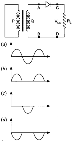
Answer/Explanation
Answer: b
Explaination:
(b) Half wave rectifier rectifies only the half cycle of the input ac signal and it blocks the other half.
9. A full-wave rectifier circuit along with the input and output voltages is shown in the figure The contribution to output voltage from diode 2 is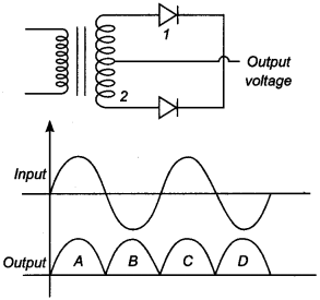
(a) A, C
(b) B, D
(c) B, C
(d) A, D
Answer/Explanation
Answer: b
Explaination:
(b) In the positive half cycle of input ac signal diode D1 is forward biased and D2 is reverse biased so in the output voltage signal, A and C are due to D1. In negative half cycle of input ac signal, D2 conducts, hence output signals B and D are due to D2
10. A 220 V AC supply is connected between points A and B (figure). What will be the potential difference V across the capacitor? [NCERT Exemplar]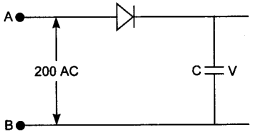
(a) 200 V
(b) 110 V
(c) 0 V
(d) 220√2 V
Answer/Explanation
Answer: d
Explaination:
(d) As p-n junction diode will conduct during positive half cycle only and during negative half cycle diode is reverse biased. During this diode will not give any output. So potential difference across the capacitor C = peak voltage of the given AC voltage.
Vo=Vrms√2 = 200√2 V.
MCQ Semiconductor Physics Question 11. In the circuit shown in figure below, if the diode forward voltage drop is 0.3 V, the voltage difference between A and B is [NCERT Exemplar]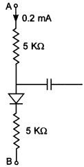
(a) 1.3 V
(b) 2.3 V
(c) 0
(d) 0.5 V
Answer/Explanation
Answer: b
Explaination:
(b) Suppose the potential difference be¬ tween A and B is VAB.
Then,VAB – 0.3
= [(r1 + r2)103] × (0.2 × 10-3) [∵ VAB=ir]
= [(5 + 5)103] × (0.2 × 10-3)
= 10 × 103 × 0.2 × 10-3 = 2
⇒ VAB = 2 + 0.3 = 2.3V
12. When an electric field is applied across a semicoriductor [NCERT Exemplar]
(a) holes move from lower energy level to higher energy level in the conduction band.
(b) electrons move from higher energy level to lower energy level in the conduction band.
(c) holes in the valence band move from higher energy level to lower energy level.
(d) holes in the valence band move from lower energy level to higher energy level.
Answer/Explanation
Answer: c
Explaination:
(c) When electric field is applied across a semiconductor, the electrons in the con-duction band move from lower energy level to higher energy level. While the holes in valence band move from higher energy level to lower energy level, where they will be having more energy.
13. At absolute zero, Si acts as a
(a) metal
(b) semiconductor
(c) insulator
(d) none of these
Answer
Answer: c
14. In good conducrors of electricity the type of bonding that exist is
(a) Van der Walls
(b) covalent
(c) ionic
(d) metallic
Answer
Answer: d
15. The manifestation of band structure in solids is due to
(a) Heisenberg uncertainty priniciple
(b) Pauli’s exclusion principle
(c) Bohr’s correspondence principle
(d) Boltzmann law
Answer
Answer: b
16. The probability of electrons to be found in the conduction band of an intrinsic semiconductor of finite temperature
(a) increases exponentially with increasing band gaP
(b) decreases exponentially with increasing band gap
(c) decreases with increasing temperature.
(d) is independent of the temperature and band gap
Answer
Answer: b
17. In an n-type silicon, which of the following statements is true.
(a) Electrons are majority carriers and trivalent atoms are the dopants’
(b) Electrons are minority carriers and pentava- lent atoms are the dopants.
(c) Holes are minority carriers and pentavalent atoms are the dopants.
(d) Holes are majority carriers and trivalent atoms are the dopants.
Answer
Answer: c
18. If a small amount of antimony is added to germanium crystal
(a) its resistance is increased
(b) it becomes a p-type semiconductor
(c) there will be more free electrons than holes in the semiconductor,
(d) none of these.
Answer
Answer: c
Semiconductor Electronics Question 19. The dominant mechanism for motion of charge carriers in forward and reverse biased silicon p-n junction are
(a) drift in forward bias, diffusion in reverse bias
(b) diffusion in forward bias, drift in reverse bias
(c) diffusion in both forward and reverse bias
(d) drift in both forward and reverse bias
Answer
Answer: b
20. In an unbiased p-n junction, holes diffuse from the p-region to n-region because
(a) free electrons in the n-region attract them
(b) they move across the junction by the potential difference
(c) hole concentration in p-region is more as compared to u-region.
(d) all of these
Answer
Answer: c
21. Region without free electrons and holes in a p-n junction is
(a) n-region
(b) p-region
(c) depletion region
(d) none of these
Answer
Answer: c
22. Which of the following statements is incorrect for the depletion region of a diode?
(a) There the mobile charges exist.
(b) Equal number of holes and electrons exist, making the region neutral.
(c) Recombination of holes and electrons has taken place.
(d) None of these
Answer
Answer: a
23. Potential barrier developed in a junction diode opposes the flow of
(a) minority carrier in both regions only
(b) majority carriers only
(c) electrons in p region
(d) holes in p region
Answer
Answer: b
24. The breakdown in a reverse biased p-n junction diode is more likely to occur due to
(a) large velocity of the minority charge carriers if the doping concentration is small
(b) large velocity of the minority charge carriers if the doping concentration is large
(c) strong electric field in a depletion region if the doping concentration is small
(d) none of these
Answer
Answer: b
25. What happens during regulation action of a Zener diode?
(a) The current through the series resistance (Rs) changes.
(b) The resistance offered by the Zener changes.
(c) The Zener resistance is constant.
(d) Both (a) and (b)
Answer
Answer: d
26. A zener diode is specified as having a breakdown voltage of 9.1 V, with a maximum power dissipation of 364 mW. What is the maximum current the diode can handle?
(a) 40 mA
(b) 60 mA
(c) 50 mA
(d) 45 mA
Answer
Answer: a
27. In a half wave rectifier circuit operating from 50 Hz mains frequency, the fundamental frequency in the ripple would be
(a) 25 Hz
(b) 50 Hz
(c) 70.7 Hz
(d) 100 Hz
Answer
Answer: b
28. In the circuit shown if current for the diode is 20 μA, the potential difference across the diode is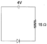
(a) 2 V
(b) 4.5 V
(c) 4 V
(d) 2.5 V
Answer
Answer: c
29. Carbon, silicon and germanium have four valence electrons each. These are characterised by valence and conduction bands separated by energy band gap respectively equal to (E^)c, (Eg)Si and (Eg)Ge. Which of the following statements is true?
(a) (Eg)Si < (Eg)Ge < (Eg)C
(b) (Eg)C< (Eg)Ge < (Eg)Si
(c) (Eg)C < (Eg)Si < (Eg)Ge
(d) (Eg)C = (Eg)Si < (Eg)Ge
Answer
Answer: c
30. If the energy of a photon of sodium light (A = 589 nm) equals the band gap of semiconductor, the minimum energy required to create hole electron pair
(a) 1.1 eV
(b) 2.1 eV
(c) 3.2 eV
(d) 1.5 eV
Answer
Answer: b
31. If in a n-type semiconductor when all donor states are filled, then the net charge density in the donor states becomes
(a) 1
(b) > 1
(c) < 1, but not zero
(d) zero
Answer
Answer: b
Physics MCQs for Class 11 with Answers Pdf Question 32. The circuit has two oppositely connected ideal diodes in parallel. What is the current flowing in the circuit?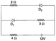
(a) 2.0 A
(b) 1.33 A
(c) 1.73 A
(d) 2.31 A
Answer
Answer: c
33. The conductivity of a semiconductor increases with increase in temperature, because
(a) number density of free current carriers increases.
(b) relaxation time increases.
(c) both number density of carriers and relaxation time increase.
(d) number density of carriers increases, relaxation time decreases but effect of decrease in relaxation time is much less than increase in number density. [NCERT Exemplar]
Answer
Answer: d
34. What happens during regulation action of a Zener diode? [NCERT Exemplar]
(a) The current in and voltage across the Zener remains fixed.
(b) The current through the series resistance (Rs) does not change.
(c) The Zener resistance is constant.
(d) The resistance offered by the Zener changes.
Answer
Answer: d
35. Silicon is a semiconductor. If a small amount of As is added to it, then its electrical conductivity _________ .
Answer/Explanation
Answer:
Explaination: increases
36. When the electrical conductivity of a semiconductor is due to the breaking of its covalent bonds, then the semiconductor is said to be ___________ .
Answer/Explanation
Answer:
Explaination: intrinsic
37. Why are the elemental dopants mainly taken from 13th and 15th group, for doping Silicon or Germanium?
Answer/Explanation
Answer:
Explaination:
The dopant has to be such that it does not distort the original pure semiconductor lattice. So that the sizes of the dopant and the semiconductor atoms should be nearly the same.
38. What is a hole? What is its physical significance?
Answer/Explanation
Answer:
Explaination:
Hole is the vacancy of electron in valence band. The vacancy with the hole behaves as an apparent free particle with effective positive charge.
39. Name one impurity each, which when added, to pure Si, produces
(i) n-type, and
(ii)p-type semiconductor.
Answer/Explanation
Answer:
Explaination:
(i) for n-type, arsenic.
(ii) for p-type, Indium.
40. Why is the conductivity of n-type semi-conductor greater than that of the p-type semi-conductor even when both of these have same level of doping?
Answer/Explanation
Answer:
Explaination:
In n-type semiconductor charge carriers are electrons and mobility of electrons is more than that of holes.
41. Name two factors on which electrical conductivity of a pure semiconductor at a given temperature depends.
Answer/Explanation
Answer:
Explaination:
(i) Band gap
(ii) Biasing.
42. What is an ideal diode?
Answer/Explanation
Answer:
Explaination:
It is a p-n junction diode which offer zero resistance in forward biasing and infinite re-sistance in reverse biasing, i.e. current flows through it in one direction only.
43. What happens to the width of depletion layer of ap-n junction when it is
(i) forward biased,
(ii) reverse biased? [AI2011]
Answer/Explanation
Answer:
Explaination:
(i) The width of depletion layer decreases.
(ii) The width of depletion layer increases.
44. What do you understand by a dynamic resistance of p-n junction diode.
Answer/Explanation
Answer:
Explaination:
Dynamic resistance is the ratio of a small change in voltage ΔV to a small change in current ΔI, i.e.\(\frac{\Delta V}{\Delta I}\).
45. Name the junction diode whose I – V characteristics are drawn below. [Delhi 2017]
Answer/Explanation
Answer:
Explaination: Solar cell.
46. State the reason, why GaAs is most commonly used in making of a solar cell.
Answer/Explanation
Answer:
Explaination: It has higher absorption coefficient.
47. Name the type of biasing of a p-n junction diode so that the junction offers very high resistance.
Answer/Explanation
Answer:
Explaination: Reverse biasing.
48. What is internal field emission?
Answer/Explanation
Answer:
Explaination:
The emission of electrons from the host atoms present in the p-n junction due to the high electric field is known as internal field emission or field ionisation.
Semiconductor Class Question 49. Why is a typical solar cell drawn in fourth quadrant?
Answer/Explanation
Answer:
Explanation:
I – V characteristics of solar cell is drawn in the fourth quadrant because a solar cell does not draw current but supplies the same to the load.
50. Why are materials like CdS or CdSe (Eg ~ 2.4 eV) not used for the fabrication of a solar cell?
Answer/Explanation
Answer:
Explaination:
Materials like CdS or CdSe (Eg ~ 2.4 eV) are not used because they will use only the high energy component of the solar energy for photo-conversion and a significant part of energy will be of no use.
Semiconductor Electronics: Materials, Devices and Simple Circuits Class 12 MCQs Questions with Answers
Question 1.
In a semiconductor, the forbidden energy gap between the valence band and the conduction band is of the order of:
(a) 1 Mev
(b) 1 ev
(c) 0.1 Mev
(d) 5ev
Answer
Answer: (b) 1 ev
Question 2.
If the conductivity of a semiconductor is only due to break of the covalent band due to the thermal excitation, then the semiconductor is called:
(a) intrinsic
(b) extrinsic
(c) Acceptor
(d) none of these
Answer
Answer: (a) intrinsic
Question 3.
In a good conductor, the energy levels in a valence band:
(a) are partially filled only.
(b) overlap with conduction band only.
(c) both (a) and (b) are correct.
(d) none of these
Answer
Answer: (c) both (a) and (b) are correct.
Question 4.
A hole in a p-type semiconductor is-
(a) an excess electron
(b) A missing atom
(c) A missing electron
(d) A donor level.
Answer
Answer: (c) A missing electron
Question 5.
The mobility of conduction electrons is greater than that of holes since electrons is greater than that of holes since electrons.
(a) are negatively charged.
(b) are lighter
(c) require smaller energy for moving through the crystal lattice.
(d) Undergo smaller number of collisions.
Answer
Answer: (c) require smaller energy for moving through the crystal lattice.
Question 6.
The Voltage gain is highest for
(a) common emitter amplifier
(b) common base amplifier
(c) common collector amplifier.
(d) Equal in all the three.
Answer
Answer: (a) common emitter amplifier
Question 7.
In an n-p-n transistor circuit the collector current is 18 mA. If 90% of the electrons emitted reach the collector, than the emitter current is:
(a) 1.6 mA
(b) 16.4 mA
(c) 18 mA
(d) 20 mA
Answer
Answer: (c) 18 mA
Question 8.
In the common emitter amplifier, the phase difference between the input voltage and output voltage signal across the collector and emitter is:
(a) 0
(b) \(\frac {π}{2}\)
(c) π
(d) \(\frac {π}{4}\)
Answer
Answer: (c) π
Question 9.
In common base amplifier, the phase difference between the input and output voltage signal is
(a) 0
(b) \(\frac {π}{2}\)
(c) \(\frac {π}{4}\)
(d) π
Answer
Answer: (a) 0
Question 10.
The part of the transistor which is heavily doped to produce a large number of majority carriers is:
(a) emitter
(b) base
(c) collector
(d) none
Answer
Answer: (a) emitter
Question 11.
In principle, Boolean algerbra is based on:
(a) simple numbers
(b) binary numbers
(c) logic
(d) truth
Answer
Answer: (c) logic
Question 12.
The following logic symbol is equivalent to: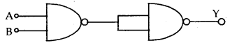
(a) AND gate
(b) OR gate
(c) NOT gate
(d) NAND gate
Answer
Answer: (a) AND gate
Question 13.
Which of the following gates corresponds to the truth table given here: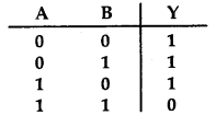
(a) NAND
(b) OR
(c) NOR
(d) AND
Answer
Answer: (a) NAND
Question 14.
The conductivity of semiconductors like Ge and Si:
(a) increases when it is doped with pentavalent impurity.
(b) increases when it is doped with trivalent impurity.
(c) increases when it is doped with pentavalent or trivalent impurity.
(d) none
Answer
Answer: (c) increases when it is doped with pentavalent or trivalent impurity.
Question 15.
In which case is the junction diode forward biased.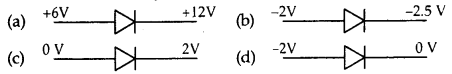
Answer
Answer: (b)
Question 16.
Assuming that the junction diode is ideal, the current in the arrangement shown here is:![]()
(a) 2 mA
(b) 30 mA
(c) 20 mA
(d) 10 mA
Answer
Answer: (c) 20 mA
Question 17.
An oscillator is an amplifier with:
(a) a large gain
(b) Negative feedback
(c) positive feedback
(d) no feedback
Answer
Answer: (c) positive feedback
Question 18.
How many AND gates are required to form, NAND gate?
(a) 0
(b) 1
(c) 2
(d) 4
Answer
Answer: (b) 1
Question 19.
Which of following statements is not true?
(a) Resistance of an intrinsic semiconductor decreases with increase in temperature.
(b) Doping pure Si with trivalent impurities gives p-type semiconductor.
(c) The majority carriers in n-type semiconductor are holes.
(d) A p-n junction can act as semiconductor diode.
Answer
Answer: (c) The majority carriers in n-type semiconductor are holes.
Question 20.
For a transistor, current amplification factor is 0.8. The transistor is changed to common emitter configuration. For a change of 6 mA in base current. Change in collector current is
(a) 4.8 mA
(b) 6 mA
(b) 8 mA
(d) 24 mA
Answer
Answer: (d) 24 mA
Question 21.
A truth table is given below. Which of the following has this type of truth table?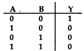
(a) XOR gate
(b) NOR gate
(b) AND gate
(d) OR gate
Answer
Answer: (b) NOR gate
Fill in the Blanks
Question 1.
…………………. is called as junction in p-n junction diode.
Answer
Answer: The surface of contact of p-type and n-type crystal.
Question 2.
The thickness of the depletion layer is of the order of ………………….
Answer
Answer: 1 µm = 10-6 m.
Question 3.
The potential barrier for S1 is about …………………. and the electric field across the junction is about ………………….
Answer
Answer: 0.7V, 7 × 10³Vm-1
Question 4.
The width of the depletion layer and the potential barrier across the junction …………………. due to reverse biasing.
Answer
Answer: increases.
Question 5.
The direction of conventional current in a p-n junction is from …………………. when it is forward biased.
Answer
Answer: p to n region.
Question 6.
The zener voltage can have value from …………………. to …………………. volts.
Answer
Answer: 1V, several hundred.
Question 7.
The arrow in the symbol of a transistor shows the direction ………………….
Answer
Answer: Conventional current or hole current.
Question 8.
Below knee voltage, the variation of current in the p-n junction is …………………. and above it, it is ………………….
Answer
Answer: non-linear, linear.
Question 9.
Various components such as resistors, inductors, capacitors, transistors, diodes and logic-gates etc. are grown over one ………………….
Answer
Answer: Semiconductor chip
Question 10.
…………………. is the most developing area where semiconductors are used.
Answer
Answer: Computer
Question 11.
1 and 0 are called ………………….
Answer
Answer: bits.
Question 12.
The connection between logic and mathematics was realised by …………………. and the algebra developed by him based on 0 and 1 is called ………………….
Answer
Answer: Boole, Boolean Algebra.
Question 13.
When a p-n junction is forward biased, then the motion of charge carriers across the barrier is due to …………………. and when it is reversed biased, then the motion of charge carriers is due to ………………….
Answer
Answer: diffusion, drift.
Question 14.
Digital circuits can be obtained by repetitive use of …………………. gates and are called digital building blocks.
Answer
Answer: NAND and NOR
Question 15.
In a digital circuit, the diodes and transistors are operated by a 5V supply. The states 1 and 0 will correspond to …………………. V and …………………. V respectively.
Answer
Answer: 5, 0
Question 16.
In insulator, the valence elctrons form a band that is ………………….
Answer
Answer: valence band which is filled completely.
Question 17.
In the band structure of an intrinsic semiconductor is located ………………….
Answer
Answer: midway between the valence band and the conduction band.
Question 18.
The region near the junction of pn—diode where there are no charge carriers is called ………………….
Answer
Answer: depletion region
Question 19.
A small impurity is added to Ge to get a p-type semiconductor and this impurity is called ………………….
Answer
Answer: trivalent.
Question 20.
The Boolean expression for AND gate is ………………….
Answer
Answer: y = A.B
Question 21.
The current gain of common emitter transistor amplifier is …………………. than one and …………………. one for common base amplifier.
Answer
Answer: more, less.