Structure 2.2.7 — Covalent Network Structures & Allotropes
Covalent Network Structures
Carbon and silicon can form extensive covalent network structures where atoms are bonded by strong covalent bonds in a continuous three-dimensional lattice. These networks result in unique physical properties due to the strength and directionality of the covalent bonds.

- Carbon (Diamond) – Each carbon atom forms 4 single covalent bonds in a tetrahedral structure.
- Silicon – Like carbon in diamond, each silicon atom also bonds to 4 others tetrahedrally to form a giant network.
Properties of Covalent Networks
- High melting and boiling points – A large amount of energy is required to break the many strong covalent bonds.
- Hardness – These structures are extremely hard (e.g. diamond is the hardest known natural substance).
- Electrical conductivity – Diamond and silicon are poor conductors because electrons are localized in bonds; graphite (another allotrope of carbon), however, conducts due to delocalized electrons.
- Insolubility – Covalent networks are insoluble in water and organic solvents because there are no interactions strong enough to overcome the covalent lattice.
Structures and Properties of Silicon, Silicon Dioxide, and Carbon Allotropes
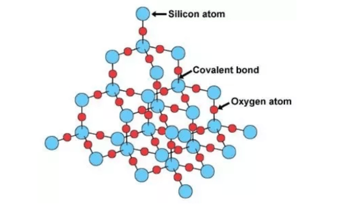
Silicon:
Structure: Each silicon atom forms four single covalent bonds arranged tetrahedrally, creating a giant covalent network (similar to diamond).
Properties:
- High melting point – due to strong covalent bonds throughout the lattice.
- Hard and brittle – rigid 3D network.
- Semi-conductor – limited conductivity increases with temperature or doping.
Uses: Microelectronics (e.g. computer chips), solar cells.
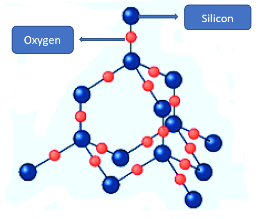
Silicon Dioxide (SiO₂) – Quartz
Structure: Each silicon atom is covalently bonded to four oxygen atoms, forming a giant 3D covalent network. Each oxygen is bonded to two silicon atoms.
Properties:
- Very high melting point – due to strong Si-O bonds throughout the structure.
- Hard and rigid – strong directional bonding.
- Insoluble in water and most solvents.
- Electrical insulator in solid state – no free electrons or mobile ions.
Uses: Glass, ceramics, optical fibers.
Allotropes of Carbon
(a) Diamond
Structure: Each carbon atom is covalently bonded tetrahedrally to four others in a giant 3D lattice.
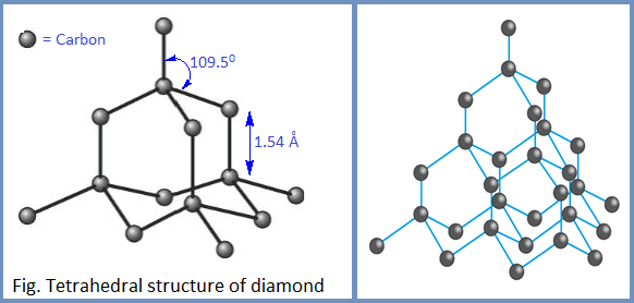
Properties:
- Extremely high melting point – strong covalent bonds throughout.
- Very hard – used in cutting tools.
- Does not conduct electricity – no delocalized electrons.
- Transparent – strong rigid lattice does not absorb visible light.
(b) Graphite
Structure: Each carbon forms three bonds in a hexagonal planar layer; layers are held together by weak van der Waals forces. One electron per carbon is delocalized.
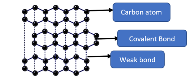
Properties:
- Good electrical conductivity – due to delocalized electrons within layers.
- Soft and slippery – layers slide easily over each other.
- High melting point – covalent bonds within layers are strong.
Uses: Lubricants, pencils, electrodes.
(c) Graphene
Structure: A single layer of carbon atoms in a hexagonal lattice (one atomic layer of graphite).
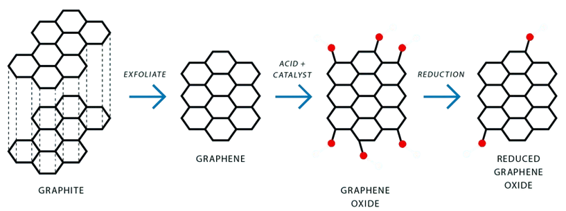
Properties:
- Extremely strong and flexible – strong covalent bonds.
- Excellent conductor of electricity and heat – delocalized electrons move freely.
- Transparent and ultra-thin.
Uses: Flexible electronics, composites, sensors.
(d) Fullerenes (e.g. \( \text{C}_{60} \))
Structure: Molecules of carbon shaped like hollow spheres or tubes; \( \text{C}_{60} \) consists of 60 carbon atoms in a structure similar to a soccer ball (20 hexagons and 12 pentagons).
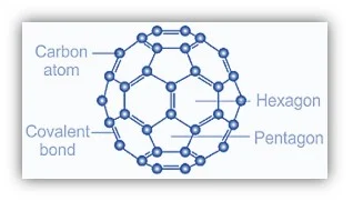
Properties:
- Low melting point compared to diamond/graphite – held together by weak intermolecular forces.
- Semi-conductive – electrons are somewhat delocalized.
- Insoluble in water – but soluble in some organic solvents.
Uses: Drug delivery systems, nanotechnology, superconductors.
Quick Revision Table
| Substance | Structure | Conductivity | Melting Point | Hardness | Key Uses |
|---|---|---|---|---|---|
| Diamond | 3D tetrahedral | No | Very high | Very hard | Cutting, jewellery |
| Graphite | Layered hexagonal | Yes | High | Soft (slippery) | Pencils, electrodes |
| Graphene | Single hexagonal layer | Excellent | Very high | Strong & flexible | Electronics, sensors |
| Fullerenes | Molecular (C₆₀ etc.) | Semi-conductor | Lower | Soft | Nanotech, medicine |
| Silicon | 3D tetrahedral | Semi-conductor | High | Hard | Chips, solar cells |
| Silicon Dioxide | 3D Si–O lattice | No | Very high | Hard | Glass, ceramics |
Example
Diamond and graphite are both allotropes of carbon. Explain the difference in their structure and relate it to their physical properties.
▶️Answer/Explanation
- Diamond: Each carbon atom forms 4 single covalent bonds in a 3D tetrahedral lattice. Strong covalent bonds throughout the structure → very high melting point, extremely hard, does not conduct electricity (no free electrons).
- Graphite: Each carbon forms 3 covalent bonds in flat layers of hexagons. Delocalized electrons exist between layers → good electrical conductivity. Layers are held by weak van der Waals forces → soft and slippery, used as a lubricant.
Example
Describe the bonding and structure in silicon dioxide and explain its physical properties such as melting point and electrical conductivity.
▶️Answer/Explanation
- Silicon dioxide (quartz) has a giant covalent structure where each silicon atom is covalently bonded to 4 oxygen atoms in a tetrahedral arrangement.
- Each oxygen bridges two silicon atoms → extensive 3D network of strong Si–O covalent bonds.
- Melting point: Very high due to the energy required to break the covalent bonds.
- Electrical conductivity: Poor conductor in solid or molten state – no delocalized electrons or mobile ions.
Example
Compare the structures and properties of graphene and fullerene \( \text{C}_{60} \). Include two differences in their bonding and conductivity.
▶️Answer/Explanation
- Graphene: A single layer of carbon atoms in a hexagonal planar lattice. Each carbon forms 3 bonds with delocalized electrons → excellent electrical conductor.
- Fullerene \( \text{C}_{60} \): Consists of 60 carbon atoms in a spherical structure made of pentagons and hexagons. Has localized bonding and only weak intermolecular forces → poor conductor compared to graphene.
- Differences:
- Graphene has a continuous sheet with delocalized electrons across the surface; \( \text{C}_{60} \) has localized π bonding within discrete molecules.
- Graphene conducts electricity much better; \( \text{C}_{60} \) is a semi-conductor at best.